- 您現(xiàn)在的位置:買賣IC網(wǎng) > PDF目錄373086 > K8D1716UTC-FI07 (SAMSUNG SEMICONDUCTOR CO. LTD.) 16M Bit (2M x8/1M x16) Dual Bank NOR Flash Memory PDF資料下載
參數(shù)資料
| 型號(hào): | K8D1716UTC-FI07 |
| 廠商: | SAMSUNG SEMICONDUCTOR CO. LTD. |
| 英文描述: | 16M Bit (2M x8/1M x16) Dual Bank NOR Flash Memory |
| 中文描述: | 1,600位(200萬(wàn)x8/1M x16)的雙銀行NOR閃存 |
| 文件頁(yè)數(shù): | 26/41頁(yè) |
| 文件大小: | 684K |
| 代理商: | K8D1716UTC-FI07 |
第1頁(yè)第2頁(yè)第3頁(yè)第4頁(yè)第5頁(yè)第6頁(yè)第7頁(yè)第8頁(yè)第9頁(yè)第10頁(yè)第11頁(yè)第12頁(yè)第13頁(yè)第14頁(yè)第15頁(yè)第16頁(yè)第17頁(yè)第18頁(yè)第19頁(yè)第20頁(yè)第21頁(yè)第22頁(yè)第23頁(yè)第24頁(yè)第25頁(yè)當(dāng)前第26頁(yè)第27頁(yè)第28頁(yè)第29頁(yè)第30頁(yè)第31頁(yè)第32頁(yè)第33頁(yè)第34頁(yè)第35頁(yè)第36頁(yè)第37頁(yè)第38頁(yè)第39頁(yè)第40頁(yè)第41頁(yè)
FLASH MEMORY
K8D1716UTC / K8D1716UBC
Revision 1.0
December 2004
26
AC CHARACTERISTICS
Read Operations
AC TEST CONDITION
Parameter
Value
Input Pulse Levels
0V to Vcc
Input Rise and Fall Times
5ns
Input and Output Timing Levels
Vcc/2
Output Load
C
L
= 30pF
Note :
1. Not 100% tested.
Parameter
Symbol
V
CC
=2.7V~3.6V
Unit
-7
-8
-9
Min
Max
Min
Max
Min
Max
Read Cycle Time (1)
t
RC
70
-
80
-
90
-
ns
Address Access Time
t
AA
-
70
-
80
-
90
ns
Chip Enable Access Time
t
CE
-
70
-
80
-
90
ns
Output Enable Time
t
OE
-
25
-
25
-
35
ns
CE & OE Disable Time (1)
t
DF
-
16
-
16
-
16
ns
Output Hold Time from Address, CE or OE (1)
t
OH
0
-
0
-
0
-
ns
Notes :
1. The I
CC
current listed includes both the DC operating current and the frequency dependent component(at 5 MHz).
The read current is typically 14 mA (@ VCC=3.0V , OE at VIH.)
2. I
CC
active during Internal Routine(program or erase) is in progress.
3. I
CC
active during Read while Write is in progress.
4. The high voltage ( V
HH
or V
ID
) must be used in the range of Vcc = 3.0V
±
0.3V
5. Not 100% tested.
6. Typical value are measured at Vcc = 3.0V,T
A
=25
°
C , Not 100% tested.
CAPACITANCE
(T
A
= 25
°
C, V
CC
= 3.3V, f = 1.0MHz)
Note
: Capacitance is periodically sampled and not 100% tested.
Item
Symbol
Test Condition
Min
Max
Unit
Input Capacitance
C
IN
V
IN
=0V
-
10
pF
Output Capacitance
C
OUT
V
OUT
=0V
-
10
pF
Control Pin Capacitance
C
IN2
V
IN
=0V
-
10
pF
Parameter
Symbol
Test Conditions
Min
Typ
Max
Unit
Voltage for Autoselect and
Block Protect (4)
Output Low Level
V
ID
V
CC
= 3.0V
±
0.3V
8.5
-
12.5
V
V
OL
I
OL
=100
μ
A, V
CC
=V
CCmin
-
-
0.4
V
Output High Level
V
OH
I
OH
=-100
μ
A, Vcc = V
CCmin
V
CC
-0.4
-
-
V
Low Vcc Lock-out Voltage (5)
V
LKO
1.8
-
2.5
V
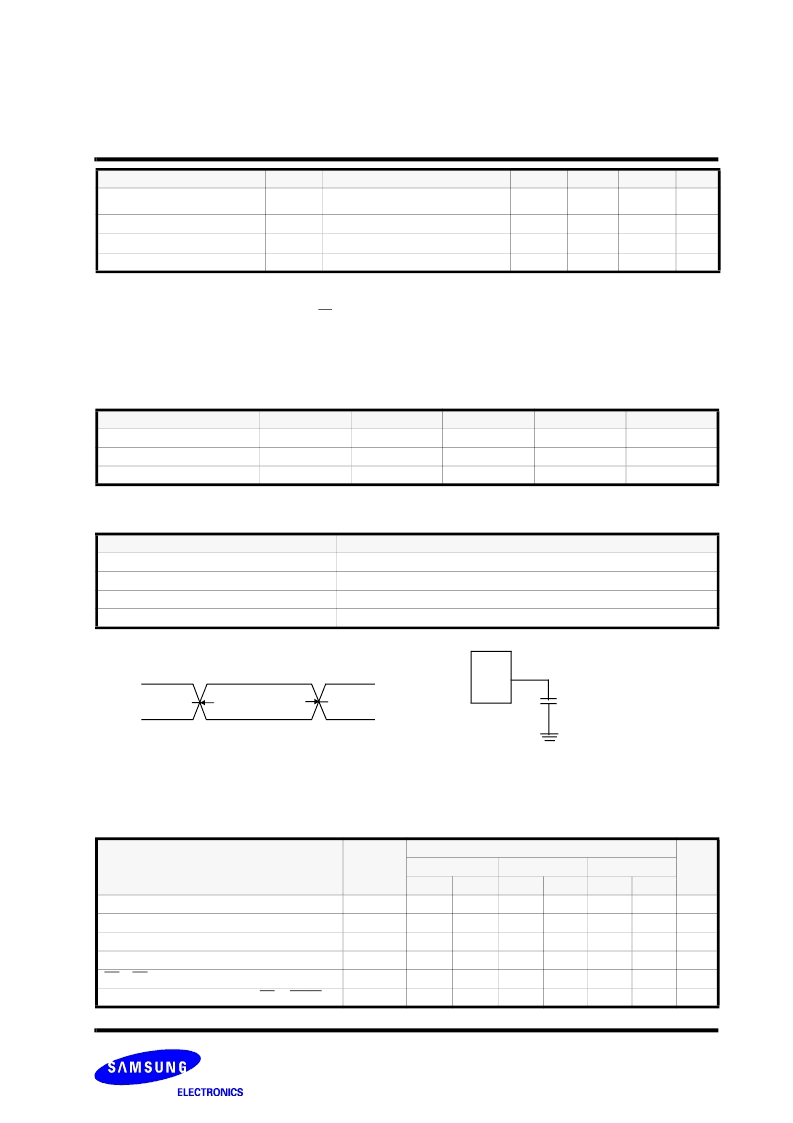
0V
Vcc
Vcc/2
Vcc/2
Input Pulse and Test Point
Input & Output
Test Point
Output Load
*
CL= 30pF including Scope
and Jig Capacitance
C
L
Device
相關(guān)PDF資料 |
PDF描述 |
|---|---|
| K8D1716UTC-FI08 | 16M Bit (2M x8/1M x16) Dual Bank NOR Flash Memory |
| K8D1716UTC-FI09 | 16M Bit (2M x8/1M x16) Dual Bank NOR Flash Memory |
| K8D1716UTC-PC07 | 16M Bit (2M x8/1M x16) Dual Bank NOR Flash Memory |
| K8D1716UTC-PC08 | 16M Bit (2M x8/1M x16) Dual Bank NOR Flash Memory |
| K8D1716UTC-PC09 | 16M Bit (2M x8/1M x16) Dual Bank NOR Flash Memory |
相關(guān)代理商/技術(shù)參數(shù) |
參數(shù)描述 |
|---|---|
| K8D1716UTC-FI08 | 制造商:SAMSUNG 制造商全稱:Samsung semiconductor 功能描述:16M Bit (2M x8/1M x16) Dual Bank NOR Flash Memory |
| K8D1716UTC-FI09 | 制造商:SAMSUNG 制造商全稱:Samsung semiconductor 功能描述:16M Bit (2M x8/1M x16) Dual Bank NOR Flash Memory |
| K8D1716UTC-PC07 | 制造商:SAMSUNG 制造商全稱:Samsung semiconductor 功能描述:16M Bit (2M x8/1M x16) Dual Bank NOR Flash Memory |
| K8D1716UTC-PC08 | 制造商:SAMSUNG 制造商全稱:Samsung semiconductor 功能描述:16M Bit (2M x8/1M x16) Dual Bank NOR Flash Memory |
| K8D1716UTC-PC09 | 制造商:SAMSUNG 制造商全稱:Samsung semiconductor 功能描述:16M Bit (2M x8/1M x16) Dual Bank NOR Flash Memory |
發(fā)布緊急采購(gòu),3分鐘左右您將得到回復(fù)。