- 您現(xiàn)在的位置:買賣IC網(wǎng) > PDF目錄373086 > K8D1716UTC-FI07 (SAMSUNG SEMICONDUCTOR CO. LTD.) 16M Bit (2M x8/1M x16) Dual Bank NOR Flash Memory PDF資料下載
參數(shù)資料
| 型號: | K8D1716UTC-FI07 |
| 廠商: | SAMSUNG SEMICONDUCTOR CO. LTD. |
| 英文描述: | 16M Bit (2M x8/1M x16) Dual Bank NOR Flash Memory |
| 中文描述: | 1,600位(200萬x8/1M x16)的雙銀行NOR閃存 |
| 文件頁數(shù): | 14/41頁 |
| 文件大小: | 684K |
| 代理商: | K8D1716UTC-FI07 |
第1頁第2頁第3頁第4頁第5頁第6頁第7頁第8頁第9頁第10頁第11頁第12頁第13頁當(dāng)前第14頁第15頁第16頁第17頁第18頁第19頁第20頁第21頁第22頁第23頁第24頁第25頁第26頁第27頁第28頁第29頁第30頁第31頁第32頁第33頁第34頁第35頁第36頁第37頁第38頁第39頁第40頁第41頁
FLASH MEMORY
K8D1716UTC / K8D1716UBC
Revision 1.0
December 2004
14
Read While Write
The K8D1716U provides dual bank memory architecture that divides the memory array into two banks. The device is capable of
reading data from one bank and writing data to the other bank simultaneously. This is so called the Read While Write operation with
dual bank architecture; this feature provides the capability of executing the read operation during Program/Erase or Erase-Suspend-
Program operation.
The Read While Write operation is prohibited during the chip erase operation. It is also allowed during erase operation when either
single block or multiple blocks from same bank are loaded to be erased. It means that the Read While Write operation is prohibited
when blocks from Bank1 and another blocks from Bank2 are loaded all together for the multi-block erase operation.
Block Group Protection & Unprotection
The K8D1716U feature hardware block group protection. This feature will disable both program and erase operations in any combi-
nation of twenty five block groups of memory. Please refer to Tables 10 and 11. The block group protection feature is enabled using
programming equipment at the user’s site. The device is shipped with all block groups unprotected.
This feature can be hardware protected or unprotected. If a block is protected, program or erase command in the protected block will
be ignored by the device. The protected block can only be read. This is useful method to preserve an important program data. The
block group unprotection allows the protected blocks to be erased or programed. All blocks must be protected before unprotect oper-
ation is executing. The block group protection and unprotection can be implemented by two methods.
The first method
needs the following conditions.
Operation
CE
OE
WE
BYTE
A9
A6
A1
A0
DQ15/
A-1
DQ8/
DQ14
DQ0/
DQ7
RESET
Block Group Protect
L
H
L
X
X
L
H
L
X
X
D
IN
V
ID
Block Group Unprotect
L
H
L
X
X
H
H
L
X
X
D
IN
V
ID
The K8D1716U needs the recovery time (20
μ
s) from the rising edge of WE in order to execute its program, erase and read opera-
tions.
Operation
CE
OE
WE
BYTE
A9
A6
A1
A0
DQ15/
A-1
DQ8/
DQ14
DQ0/
DQ7
RESET
Block Group Protect
L
V
ID
X
V
ID
L
H
L
X
X
X
H
Block Group Unprotect
L
V
ID
X
V
ID
H
H
L
X
X
X
H
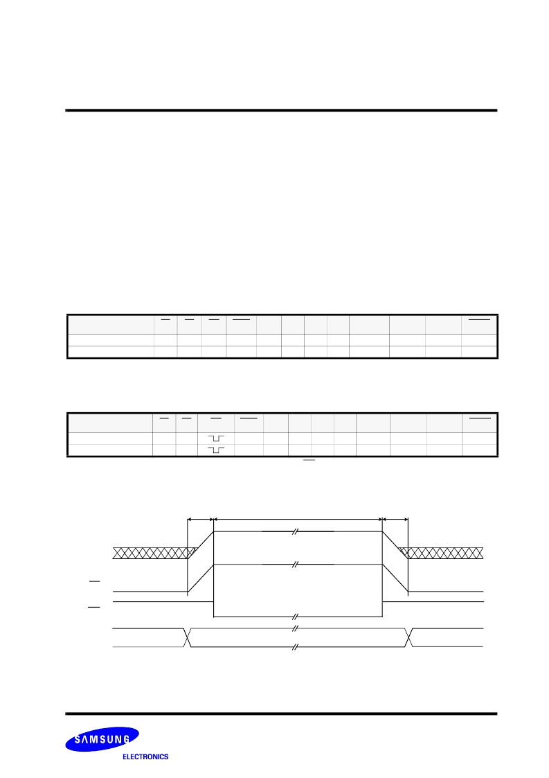
A9
OE
Don
'
t Care
WE
Address
Don
'
t Care
500ns
500ns
Block Group Address*
Figure 8. Block Group Protect Sequence (The second method)
Block Group Protect:150
μ
s
Block Group Unprotect:500ms
Notes :
* Block Group Address is Don't Care during Block Group Unprotection.
Address must be inputted to the block group address (A12~A19) during block group protection operation. Please refer to Figure 9
(Algorithm) and Switching Waveforms of Block Group Protect & Unprotect Operations.
The second method
needs the following conditions in order to keep backward compatibility. Please refer to Figure 8.
Low
V
ID
V
ID
相關(guān)PDF資料 |
PDF描述 |
|---|---|
| K8D1716UTC-FI08 | 16M Bit (2M x8/1M x16) Dual Bank NOR Flash Memory |
| K8D1716UTC-FI09 | 16M Bit (2M x8/1M x16) Dual Bank NOR Flash Memory |
| K8D1716UTC-PC07 | 16M Bit (2M x8/1M x16) Dual Bank NOR Flash Memory |
| K8D1716UTC-PC08 | 16M Bit (2M x8/1M x16) Dual Bank NOR Flash Memory |
| K8D1716UTC-PC09 | 16M Bit (2M x8/1M x16) Dual Bank NOR Flash Memory |
相關(guān)代理商/技術(shù)參數(shù) |
參數(shù)描述 |
|---|---|
| K8D1716UTC-FI08 | 制造商:SAMSUNG 制造商全稱:Samsung semiconductor 功能描述:16M Bit (2M x8/1M x16) Dual Bank NOR Flash Memory |
| K8D1716UTC-FI09 | 制造商:SAMSUNG 制造商全稱:Samsung semiconductor 功能描述:16M Bit (2M x8/1M x16) Dual Bank NOR Flash Memory |
| K8D1716UTC-PC07 | 制造商:SAMSUNG 制造商全稱:Samsung semiconductor 功能描述:16M Bit (2M x8/1M x16) Dual Bank NOR Flash Memory |
| K8D1716UTC-PC08 | 制造商:SAMSUNG 制造商全稱:Samsung semiconductor 功能描述:16M Bit (2M x8/1M x16) Dual Bank NOR Flash Memory |
| K8D1716UTC-PC09 | 制造商:SAMSUNG 制造商全稱:Samsung semiconductor 功能描述:16M Bit (2M x8/1M x16) Dual Bank NOR Flash Memory |
發(fā)布緊急采購,3分鐘左右您將得到回復(fù)。