- 您現(xiàn)在的位置:買賣IC網(wǎng) > PDF目錄374277 > K4R881869D (SAMSUNG SEMICONDUCTOR CO. LTD.) 256/288Mbit RDRAM(D-die) PDF資料下載
參數(shù)資料
| 型號(hào): | K4R881869D |
| 廠商: | SAMSUNG SEMICONDUCTOR CO. LTD. |
| 英文描述: | 256/288Mbit RDRAM(D-die) |
| 中文描述: | 256/288Mbit的RDRAM(深模) |
| 文件頁(yè)數(shù): | 14/20頁(yè) |
| 文件大小: | 311K |
| 代理商: | K4R881869D |
第1頁(yè)第2頁(yè)第3頁(yè)第4頁(yè)第5頁(yè)第6頁(yè)第7頁(yè)第8頁(yè)第9頁(yè)第10頁(yè)第11頁(yè)第12頁(yè)第13頁(yè)當(dāng)前第14頁(yè)第15頁(yè)第16頁(yè)第17頁(yè)第18頁(yè)第19頁(yè)第20頁(yè)
Direct RDRAM
K4R571669D/K4R881869D
Page 12
Version 1.4 July 2002
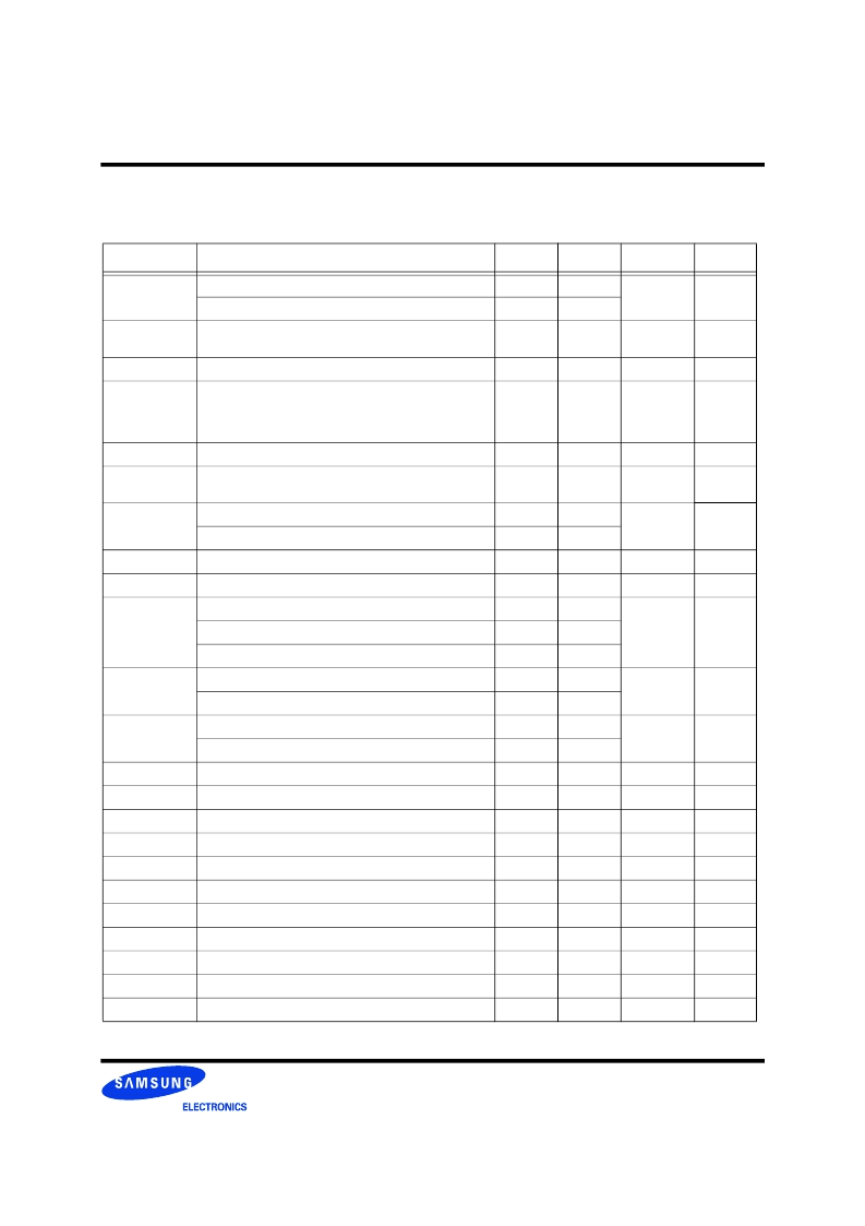
Timing Conditions
Table 11: Timing Conditions
Symbol
Parameter
Min
Max
Unit
Figure(s)
t
CYCLE
CTM and CFM cycle times (-1066)
1.875
2.5
ns
Figure 56
CTM and CFM cycle times (-800)
2.50
3.33
t
CR
, t
CF
CTM and CFM input rise and fall times. Use the minimum value of
these parameters during testing.
0.2
0.5
ns
Figure 56
t
CH
, t
CL
CTM and CFM high and low times
40%
60%
t
CYCLE
Figure 56
t
TR
CTM-CFM differential (MSE/MS=0/0)
CTM-CFM differential (MSE/MS=1/1)
a
CTM-CFM differential only for 1.875ns (MSE/MS=1/0)
0.0
0.9
-0.1
1.0
1.0
0.1
t
CYCLE
Figure 43
Figure 56
t
DCW
Domain crossing window
-0.1
0.1
t
CYCLE
Figure 62
t
DR
, t
DF
DQA/DQB/ROW/COL input rise/fall times (20% to 80%). Use the
minimum value of these parameters during testing.
0.2
0.45
ns
Figure 57
t
S
, t
H
DQA/DQB/ROW/COL-to-CFM set/hold @ t
CYCLE
=1.875ns
0.160
b
-
ns
Figure 57
DQA/DQB/ROW/COL-to-CFM set/hold @ t
CYCLE
=2.50ns
0.200
b.c
-
t
DR1,
t
DF1
SIO0, SIO1 input rise and fall times
-
5.0
ns
Figure 59
t
DR2,
t
DF2
CMD, SCK input rise and fall times
-
2.0
ns
Figure 59
t
CYCLE1
SCK cycle time - Serial control register transactions
1000
-
ns
Figure 59
SCK cycle time - Power transitions @ t
CYCLE
=1.875ns
7.5
-
SCK cycle time - Power transitions @ t
CYCLE
=2.50ns
10
-
t
CH1
, t
CL1
SCK high and low times @ t
CYCLE
=1.875ns
3.5
-
ns
Figure 59
SCK high and low times @ t
CYCLE
=2.50ns
4.25
-
t
S1
CMD setup time to SCK rising or falling edge
d
@ t
CYCLE
=1.875ns
1.0
-
ns
Figure 59
CMD setup time to SCK rising or falling edge
d
@ t
CYCLE
=2.50ns
1.25
-
t
H1
CMD hold time to SCK rising or falling edge
d
1
-
ns
Figure 59
t
S2
SIO0 setup time to SCK falling edge
40
-
ns
Figure 59
t
H2
SIO0 hold time to SCK falling edge
40
-
ns
Figure 59
t
S3
PDEV setup time on DQA5..0 to SCK rising edge.
0
-
ns
Figure 50
t
H3
PDEV hold time on DQA5..0 to SCK rising edge.
5.5
-
ns
Figure 60
t
S4
ROW2..0, COL4..0 setup time for quiet window
-1
-
t
CYCLE
Figure 50
t
H4
ROW2..0, COL4..0 hold time for quiet window
e
5
-
t
CYCLE
Figure 50
t
NPQ
Quiet on ROW/COL bits during NAP/PDN entry
4
-
t
CYCLE
Figure 49
t
READTOCC
Offset between read data and CC packets (same device)
12
-
t
CYCLE
Figure 54
t
CCSAMTOREAD
Offset between CC packet and read data (same device)
8
-
t
CYCLE
Figure 54
t
CE
CTM/CFM stable before NAP/PDN exit
2
-
t
CYCLE
Figure 50
相關(guān)PDF資料 |
PDF描述 |
|---|---|
| K4R761869A-GCN1 | 576Mbit RDRAM (A-die) 1M x 18bit x 32s banks Direct RDRAMTM |
| K4R761869A-GCT9 | 576Mbit RDRAM (A-die) 1M x 18bit x 32s banks Direct RDRAMTM |
| K4R761869A-F | 576Mbit RDRAM (A-die) 1M x 18bit x 32s banks Direct RDRAMTM |
| K4R761869A-FbCcN1 | 576Mbit RDRAM (A-die) 1M x 18bit x 32s banks Direct RDRAMTM |
| K4R761869A-FCM8 | 576Mbit RDRAM (A-die) 1M x 18bit x 32s banks Direct RDRAMTM |
相關(guān)代理商/技術(shù)參數(shù) |
參數(shù)描述 |
|---|---|
| K4R881869D-FCM8 | 制造商:Samsung Electro-Mechanics 功能描述:16M X 18 DIRECT RAMBUS DRAM, PBGA92 |
| K4R881869EFCT9 | 制造商:Samsung Semiconductor 功能描述: |
| K4R881869E-GCM8000 | 制造商:Samsung Semiconductor 功能描述:DRAM CHIP DIRECT RDRAM 288MBIT 2.5V 92PIN WBGA - Bulk |
| K4R881869E-GCM8T00 | 制造商:Samsung Semiconductor 功能描述:288MRDRAMDIRECT RDRAMX18WBGA - Tape and Reel |
| K4R881869E-GCT9000 | 制造商:Samsung Semiconductor 功能描述:288MRDRAMDIRECT RDRAMX18WBGA - Bulk |
發(fā)布緊急采購(gòu),3分鐘左右您將得到回復(fù)。