- 您現(xiàn)在的位置:買賣IC網(wǎng) > PDF目錄383186 > IXBD4411 (IXYS Corporation) MICA RoHS Compliant: No PDF資料下載
參數(shù)資料
| 型號: | IXBD4411 |
| 廠商: | IXYS Corporation |
| 英文描述: | MICA RoHS Compliant: No |
| 中文描述: | ISOSMART半橋驅(qū)動器芯片組 |
| 文件頁數(shù): | 6/11頁 |
| 文件大小: | 705K |
| 代理商: | IXBD4411 |
2004 IXYS All rights reserved
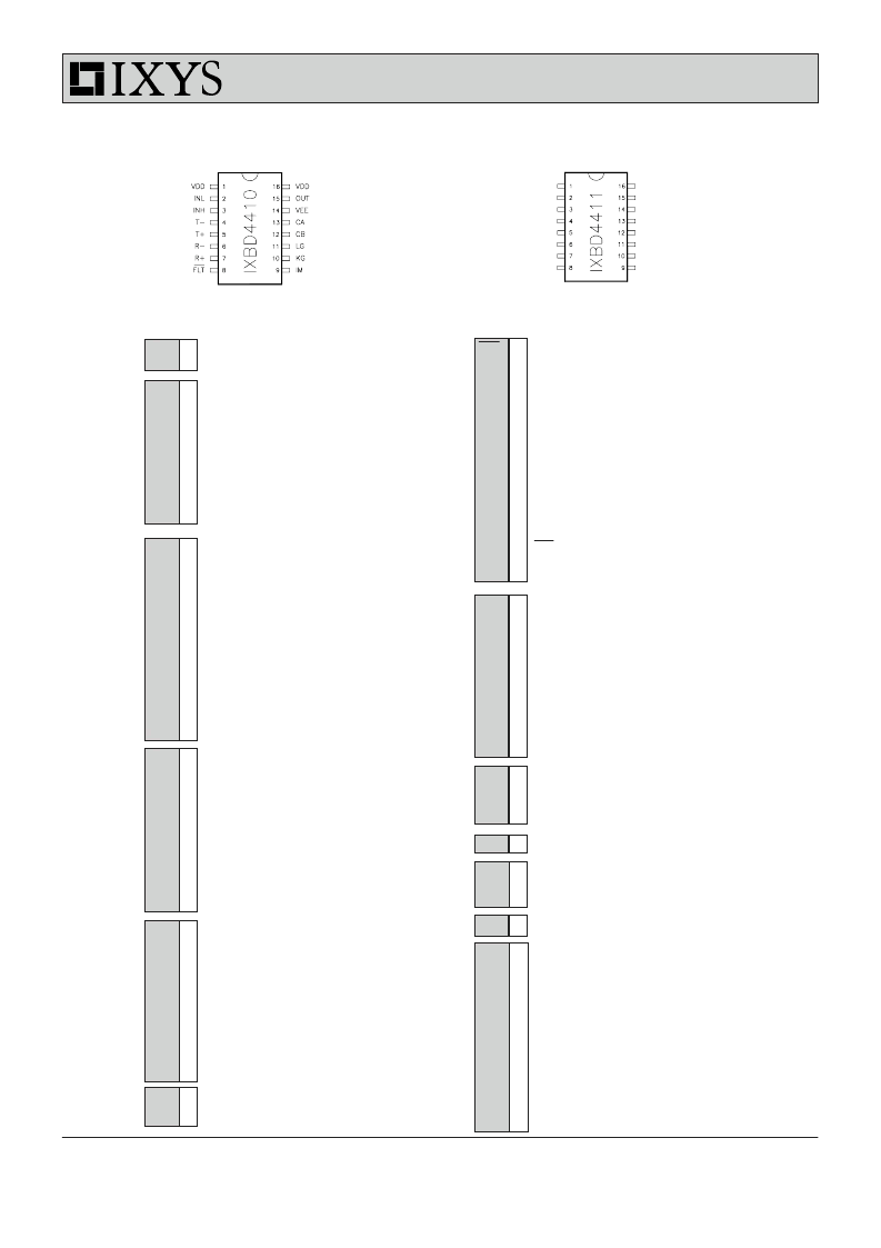
IXBD4410
IXBD4411
Pin Description
IXBD4411 (High-Side Driver)
Sym. Pin Description of IXBD 4410/4411
FLT
NC
8
Low/high side fault output. In the
IXBD4410, this output indicates
a fault condition of either device
of the chipset. A "high" indicates
no fault, A "low" indicates that
either overcurrent,V
or V
under-voltage occurred. In case
of overcurrent, this output will
remain active "low" until the next
input cycle of the respective
driver. In case of under-voltage,
this output will remain "low" until
the proper voltage is restored.
The IXBD4411 does not have a
FLT output,and its pin 8 should
be tied to LG
N
o
C
onnection (IXBD 4411)
IM
9
Current sense or desaturation
detection input. This input is
active only while the OUT pin is
"high" (on). When the OUT pin is
"low" (off) this input is pulled to
ground through a 70
resistor.
Any voltage at this pin above the
threshold of .3 V typical, will turn
the output (pin 15) off. This pin is
used for power device
overcurrent protection.
KG
10 Kelvin ground. This ground is
used as Kelvin connection for
overcurrent or desaturation
sensing.
LG
11 Logic and power ground.
CB
12 Capacitor terminals for negative
charge pump (V
); "+"
13 terminal is CB (pin 12).
CA
VEE
14 Negative supply terminal(substrate)
OUT
15 Gate drive output. In the
IXBD4410 this output responds
to the INL signal. A "high" at INL
will turn it on ("high"), a "low" will
turn it off ("low"). In the
IXBD4411, this output responds
to the transmitted signal from the
companion IXBD4410. A "high"
at INH of the IXBD4410 drives
will turn it on ("high"). A "low"
will turn it off ("low"). This output
will turn off ("low") also in
response to any fault condition.
VDD
NC
NC
T-
T+
R-
R+
NC
VDD
OUT
VEE
CA
CB
LG
KG
IM
Pin Description
IXBD4410 (Low-Side Driver)
Sym. Pin Description of IXBD 4410/4411
VDD
1
16
Positive power supply.
INL
NC
2
Logic input signal referenced to
LG (logic ground). In the
IXBD4410. A "high" to this pin
turns on its gate drive output and
resets its fault logic. A "low" to
this pin turns off the gate drive
output. In the IXBD4411 this pin
is not used and should be
connected to its ground (LG).
N
o
C
onnection (IXBD 4411)
INH
NC
3
Logic input signal referenced to
LG (logic ground). In the
IXBD4410, this signal is
transmitted to the IXBD4411
"high-side" driver through pins 4
and 5 (T- and T+). A "high" to
this pin turns on the IXBD4411
gate drive output and resets its
fault logic. A "low" to this pin
turns off the IXBD4411 gate
drive output. In the IXBD4411
this pin is not used and should
be connected to its ground (LG).
N
o
C
onnection (IXBD 4411)
T-
T+
4
5
Transmitter output complemen-
tary drive signals. Direct drive of
the low signal transformer, which
is connected to the receiver of
the chipset's companion device.
In the IXBD4410, this signal
transmits the on/off command to
its companion IXBD4411. In the
IXBD4411, this signal transmits
the fault indication to its
companion IXBD4410 driver.
R-
R+
6
7
Receiver input complementary
signal. Directly connected to the
low signal transformer, which is
driven by the chipset's compa-
nion device. In the IXBD4410,
this input receives the fault
indication from its companion
IXBD4411 driver. In the
IXBD4411, this input receives
the on/off command from its
companion IXBD4410 driver.
VEE
T
A
B
Connected to
Pin 14 (substrate)
相關(guān)PDF資料 |
PDF描述 |
|---|---|
| IXBD4411PI | MICA RoHS Compliant: No |
| IXBD4411SI | Silver Mica Capacitor; Capacitance:100pF; Capacitance Tolerance:+/- 5%; Series:CM04; Voltage Rating:500VDC; Capacitor Dielectric Material:Mica; Termination:Radial Leaded; Lead Pitch:3.6mm; Leaded Process Compatible:No RoHS Compliant: No |
| IXBF9N140 | High Voltage BIMOSFET |
| IXBF9N160 | High Voltage BIMOSFET |
| IXBH15N140 | High Voltage BIMOSFET Monolithic Bipolar MOS Transistor |
相關(guān)代理商/技術(shù)參數(shù) |
參數(shù)描述 |
|---|---|
| IXBD4411PC | 制造商:未知廠家 制造商全稱:未知廠家 功能描述:Interface IC |
| IXBD4411PI | 功能描述:功率驅(qū)動器IC 1/2Bridge2A RoHS:否 制造商:Micrel 產(chǎn)品:MOSFET Gate Drivers 類型:Low Cost High or Low Side MOSFET Driver 上升時間: 下降時間: 電源電壓-最大:30 V 電源電壓-最小:2.75 V 電源電流: 最大功率耗散: 最大工作溫度:+ 85 C 安裝風(fēng)格:SMD/SMT 封裝 / 箱體:SOIC-8 封裝:Tube |
| IXBD4411SI | 功能描述:功率驅(qū)動器IC 1/2Bridge2A RoHS:否 制造商:Micrel 產(chǎn)品:MOSFET Gate Drivers 類型:Low Cost High or Low Side MOSFET Driver 上升時間: 下降時間: 電源電壓-最大:30 V 電源電壓-最小:2.75 V 電源電流: 最大功率耗散: 最大工作溫度:+ 85 C 安裝風(fēng)格:SMD/SMT 封裝 / 箱體:SOIC-8 封裝:Tube |
| IXBD4412PC | 制造商:未知廠家 制造商全稱:未知廠家 功能描述:Interface IC |
| IXBD4412PI | 制造商:未知廠家 制造商全稱:未知廠家 功能描述:Interface IC |
發(fā)布緊急采購,3分鐘左右您將得到回復(fù)。