- 您現(xiàn)在的位置:買賣IC網(wǎng) > PDF目錄383186 > IXBD4410P (IXYS Corporation) MICA RoHS Compliant: No PDF資料下載
參數(shù)資料
| 型號(hào): | IXBD4410P |
| 廠商: | IXYS Corporation |
| 英文描述: | MICA RoHS Compliant: No |
| 中文描述: | ISOSMART半橋驅(qū)動(dòng)器芯片組 |
| 文件頁(yè)數(shù): | 7/11頁(yè) |
| 文件大小: | 705K |
| 代理商: | IXBD4410P |
7
2004 IXYS All rights reserved
IXBD4410
IXBD4411
Application
The IXBD4410/4411 chipset devices
are specifically designed as MOS-
gated transistor drivers in half-bridge
power converters, 1- and 3-phase
motor controls, and UPS applications.
The phase-leg PWM command is
normally generated by previous (user
provided) circuitry. It must be
decomposed into two separate logic
signals, one for the high-side and one
for the low-side power transistors, with
appropriate deadtime for each state
transition. The deadtime insures non-
overlapping conduction even if the
turn-on and turn-off delay times of the
power devices are unequal. The
minimum deadtime should be greater
than t
.
A separate circuit, or an IC
device like the
IXYS
deadtime
generator IXDP630, can be used to
perform this function. The
ISOSMART chipset family of
devices do not generate deadtime,
although there is an internal lockout
that prohibits one device form being
commanded "on" before the other is
commanded "off". This simplifies start-
up and shutdown protection circuitry,
preventing logic error during power-up
from turning on both high-and low-side
transistors simultaneously.
Negative V
EE
Charge Pump Circuit
Design
The on-chip V
generator provided in
the IXBD4410/4411 generates a nega-
tive power supply, regulated at 20 V
below the positive V
rail. If V
is +10
V, V
will be -10 V. If V
is +15 V, V
EE
will be -5 V. This negative drive
potential in the off-state is either
desirable or required in many in-
stances. When switching a clamped
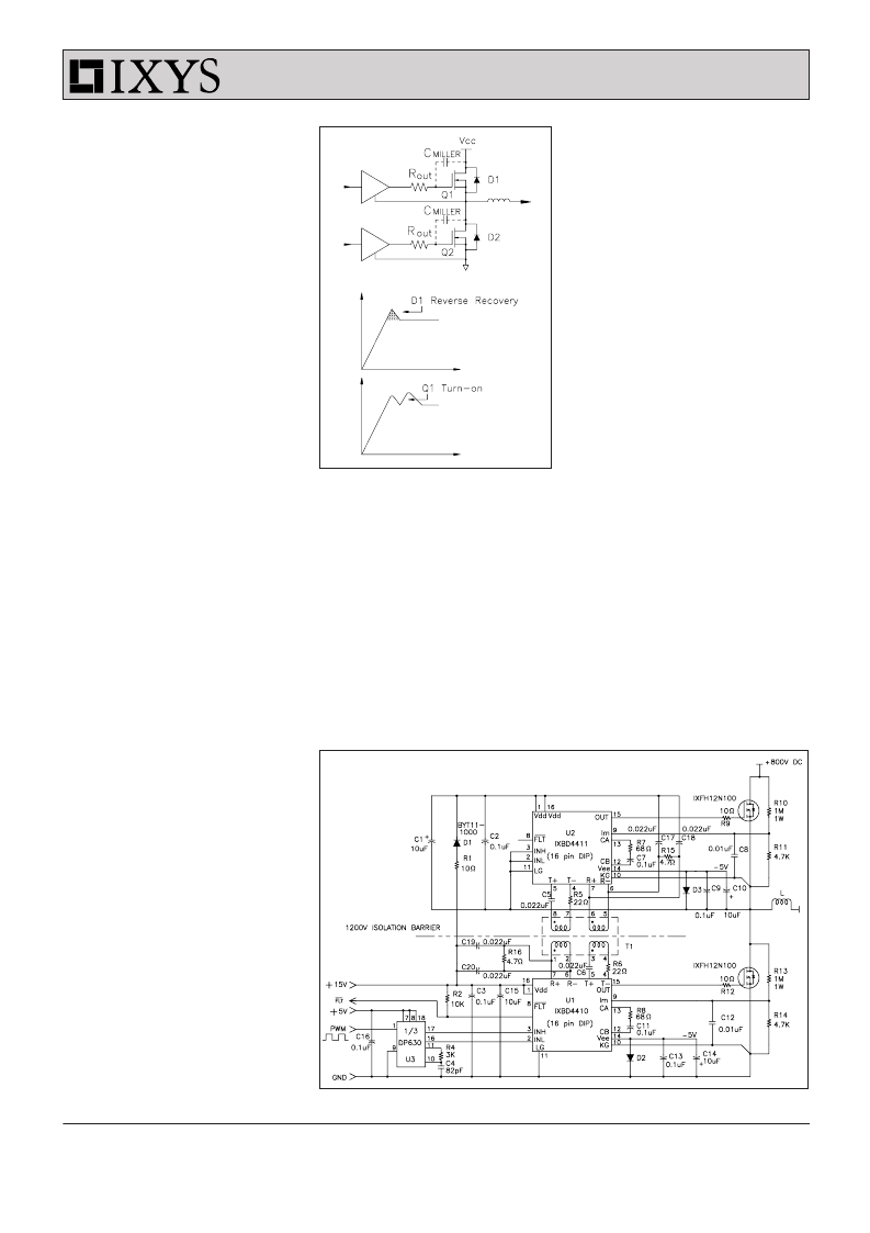
inductive load (Fig. 5), the turn-on of
Q2 will commutate the freewheeling
diode around Q1. Whether this diode is
intrinsic (as in a MOSFET) or extrinsic
(IGBT or bipolar), its reverse recovery
is critical to proper circuit operation.
At high turn-on di/dt in Q2 and near its
rated voltage, the recovery of D1 can
get quite "snappy" (the di/dt in the
second half of the recovery process,
after the diode has begun to recover its
blocking capability, can get very large),
creating a very high dv/dt across Q1.
This dv/dt is impressed across the
Miller capacitance of Q1, forcing a
large current to flow out the gate
reduces the voltage required to create
a failure, this problem is even more
likely to occur. In an industrial module
package (e.g.: a 150 A/1200 V IGBT
phase-leg module), the series induc-
tance contributed by the long gate
leads and connectors further compli-
cate the design.
In a heavily snubbered converter, or in
a power supply design with low
transformer leakage inductance, the
design problem is relatively simple and
negative drive is seldom required.
However, in a modern snubberless or
lightly snubbered converter design, it is
important to keep the gate drive
impedance high enough during
transistor turnoff to limit the reapplied
dv/dt (the transistor is its own 'active'
snubber). This is always important for
EMI control, and in the case of IGBT
may be required to achieve the
necessary RBSOA. At the same time, it
is mandatory to keep the off-state gate
drive impedance very low to assure the
transistor remain off during induced
dv/dt (including diode recovery dv/dt).
In some instances, it is simply not
possible to satisfy both criteria with 0 V
applied in the off-state. In these cases
the IXBD4410/4411 with V
negative
bias generator must be used.
The internal V
generator is a charge
pump circuit. Referring to Fig. 6, an
external charge pump capacitor is
required between the CA and CB
terminal of the device. If this current
pulse causes a high enough voltage
drop across the output impedance of
the gate drive circuit, R
out
, Q1 will be
turned on.
The Q1 conduction in every instance
Q2 is turned on (and vice versa), aside
from degrading efficiency, can lead to
catastrophic failure of both power
transistors. At high temperature, where
the -6 to -7 mV/
°
C temperature
coefficient of IGBT/MOSFET threshold
Fig. 5: Switching a clamped inductive
load
Fig. 6: IXBD4410/4411 Detailed one phase circuit with dead time generator IXDP 630
1N5817
1N5817
相關(guān)PDF資料 |
PDF描述 |
|---|---|
| IXBD4410PI | MICA RoHS Compliant: No |
| IXBD4410SI | MICA RoHS Compliant: No |
| IXBD4411 | MICA RoHS Compliant: No |
| IXBD4411PI | MICA RoHS Compliant: No |
| IXBD4411SI | Silver Mica Capacitor; Capacitance:100pF; Capacitance Tolerance:+/- 5%; Series:CM04; Voltage Rating:500VDC; Capacitor Dielectric Material:Mica; Termination:Radial Leaded; Lead Pitch:3.6mm; Leaded Process Compatible:No RoHS Compliant: No |
相關(guān)代理商/技術(shù)參數(shù) |
參數(shù)描述 |
|---|---|
| IXBD4410PC | 制造商:未知廠家 制造商全稱:未知廠家 功能描述:Interface IC |
| IXBD4410PI | 功能描述:功率驅(qū)動(dòng)器IC 1/2Bridge2A RoHS:否 制造商:Micrel 產(chǎn)品:MOSFET Gate Drivers 類型:Low Cost High or Low Side MOSFET Driver 上升時(shí)間: 下降時(shí)間: 電源電壓-最大:30 V 電源電壓-最小:2.75 V 電源電流: 最大功率耗散: 最大工作溫度:+ 85 C 安裝風(fēng)格:SMD/SMT 封裝 / 箱體:SOIC-8 封裝:Tube |
| IXBD4410SI | 功能描述:功率驅(qū)動(dòng)器IC 1/2Bridge2A RoHS:否 制造商:Micrel 產(chǎn)品:MOSFET Gate Drivers 類型:Low Cost High or Low Side MOSFET Driver 上升時(shí)間: 下降時(shí)間: 電源電壓-最大:30 V 電源電壓-最小:2.75 V 電源電流: 最大功率耗散: 最大工作溫度:+ 85 C 安裝風(fēng)格:SMD/SMT 封裝 / 箱體:SOIC-8 封裝:Tube |
| IXBD4411 | 制造商:IXYS 制造商全稱:IXYS Corporation 功能描述:ISOSMART Half Bridge Driver Chipset |
| IXBD4411PC | 制造商:未知廠家 制造商全稱:未知廠家 功能描述:Interface IC |
發(fā)布緊急采購(gòu),3分鐘左右您將得到回復(fù)。