- 您現(xiàn)在的位置:買賣IC網(wǎng) > PDF目錄10839 > ISL59424IR-T7 (Intersil)IC AMP TRIPLE MUX 1GHZ 24-QFN PDF資料下載
參數(shù)資料
| 型號: | ISL59424IR-T7 |
| 廠商: | Intersil |
| 文件頁數(shù): | 14/14頁 |
| 文件大小: | 0K |
| 描述: | IC AMP TRIPLE MUX 1GHZ 24-QFN |
| 標(biāo)準(zhǔn)包裝: | 1,000 |
| 應(yīng)用: | 2:1 多路復(fù)用器-放大器 |
| 電路數(shù): | 3 |
| -3db帶寬: | 1GHz |
| 轉(zhuǎn)換速率: | 1200 V/µs |
| 電流 - 電源: | 39mA |
| 電流 - 輸出 / 通道: | 130mA |
| 安裝類型: | 表面貼裝 |
| 封裝/外殼: | 24-VFQFN 裸露焊盤 |
| 供應(yīng)商設(shè)備封裝: | 24-QFN(5x4) |
| 包裝: | 帶卷 (TR) |
9
FN7456.3
September 30, 2011
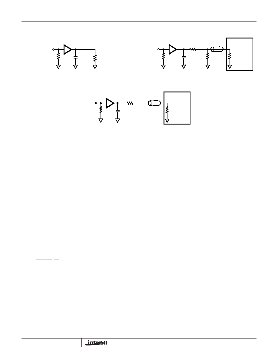
Figure 18A illustrates the optimum output load for testing AC
performance. Figure 18B illustrates the optimum output load
when connecting to 50
Ω input terminated equipment.
Application Information
General
The ISL59424, ISL59445 are triple 2:1 and 4:1 muxes that
are ideal for the matrix element of high performance
switchers and routers. The ISL59424, ISL59445 are
optimized to drive a 1.5pF in parallel with a 500
Ω load. The
capacitance can be split between the PCB capacitance an
and external load capacitance. Their low input capacitance
and high input resistance provide excellent 50
Ω or 75Ω
terminations.
Ground Connections
For the best isolation and crosstalk rejection, all GND pins
and NIC pins must connect to the GND plane.
Control Signals
S0, S1, ENABLE, LE, HIZ - These pins are binary coded,
TTL/CMOS compatible control inputs. The S0, S1 pins select
which one of the inputs connect to the output. All three
amplifiers are switched simultaneously from their respective
inputs. The ENABLE, LE, HIZ pins are used to disable the part
to save power, latch in the last logic state and three-state the
output amplifiers, respectively. For control signal rise and fall
times less than 10ns the use of termination resistors close to
the part should be considered to minimize transients coupled
to the output.
Power-Up Considerations
The ESD protection circuits use internal diodes from all pins
the V+ and V- supplies. In addition, a dV/dT- triggered clamp
is connected between the V+ and V- pins, as shown in the
Equivalent Circuits 1 through 4 section of the “Pin
Descriptions” on page 8. The dV/dT triggered clamp
imposes a maximum supply turn-on slew rate of 1V/s.
Damaging currents can flow for power supply rates-of-rise in
excess of 1V/s, such as during hot plugging. Under these
conditions, additional methods should be employed to
ensure the rate of rise is not exceeded.
Consideration must be given to the order in which power is
applied to the V+ and V- pins, as well as analog and logic
input pins. Schottky diodes (Motorola MBR0550T or
equivalent) connected from V+ to ground and V- to ground
(Figure 19) will shunt damaging currents away from the
internal V+ and V- ESD diodes in the event that the V+
supply is applied to the device before the V- supply.
If positive voltages are applied to the logic or analog video
input pins before V+ is applied, current will flow through the
internal ESD diodes to the V+ pin. The presence of large
decoupling capacitors and the loading effect of other circuits
connected to V+, can result in damaging currents through
the ESD diodes and other active circuits within the device.
Therefore, adequate current limiting on the digital and
analog inputs is needed to prevent damage during the time
the voltages on these inputs are more positive than V+.
AC Test Circuits
FIGURE 18A. TEST CIRCUIT WITH OPTIMAL OUTPUT
LOAD
FIGURE 18B. TEST CIRCUIT FOR MEASURING WITH
50Ω OR 75Ω INPUT TERMINATED
EQUIPMENT
FIGURE 18C. BACKLOADED TEST CIRCUIT FOR VIDEO CABLE APPLICATION. BANDWIDTH AND LINEARITY FOR RL
LESS THAN 500Ω WILL BE DEGRADED.
FIGURE 18. TEST CIRCUITS
ISL59424, ISL59445
CL
50Ω
VIN
500Ω
RL
1.5pF
OR
75Ω
ISL59424, ISL59445
RS
CL
VIN
475Ω
TEST
1.5pF
50Ω
OR
75Ω
50Ω
OR
75Ω
50Ω
OR
75Ω
EQUIPMENT
OR
462.5Ω
ISL59424, ISL59445
RS
CL
VIN
50Ω OR 75Ω
TEST
1.5pF
50Ω
OR
75Ω
50Ω
OR
75Ω
EQUIPMENT
ISL59424, ISL59445
相關(guān)PDF資料 |
PDF描述 |
|---|---|
| ISL59424IR-T13 | IC AMP TRIPLE MUX 1GHZ 24-QFN |
| VE-25P-IW-S | CONVERTER MOD DC/DC 13.8V 100W |
| ISL59421IU-T7 | IC AMP MULTIPLEX 865MHZ 10-MSOP |
| ISL59421IU-T13 | IC AMP MULTIPLEX 865MHZ 10-MSOP |
| ISL59421IU | IC AMP MULTIPLEX 865MHZ 10-MSOP |
相關(guān)代理商/技術(shù)參數(shù) |
參數(shù)描述 |
|---|---|
| ISL59424IRZ | 制造商:Intersil Corporation 功能描述:ANLG MUX/AMP TRIPLE 2:1 24QFN EP - Bulk 制造商:Intersil Corporation 功能描述:1GHz Triple Multiplexing Amplifiers |
| ISL59424IRZ-T13 | 制造商:Intersil Corporation 功能描述:ANLG MUX/AMP TRIPLE 2:1 24QFN EP - Tape and Reel |
| ISL59424IRZ-T7 | 制造商:Intersil Corporation 功能描述:ANLG MUX/AMP TRIPLE 2:1 24QFN EP - Tape and Reel 制造商:Intersil 功能描述:Intersil ISL59424IRZ-T7 Analog Switch Multiplexers 制造商:Intersil 功能描述:ISL80102 EVAL 2 10LD 2A BAG&SHIP IC DIFER |
| ISL59440 | 制造商:INTERSIL 制造商全稱:Intersil Corporation 功能描述:400MHz Multiplexing Amplifier |
| ISL59440_07 | 制造商:INTERSIL 制造商全稱:Intersil Corporation 功能描述:400MHz Multiplexing Amplifier |
發(fā)布緊急采購,3分鐘左右您將得到回復(fù)。