- 您現(xiàn)在的位置:買賣IC網(wǎng) > PDF目錄360957 > IRHF7310 PDF資料下載
參數(shù)資料
| 型號(hào): | IRHF7310 |
| 文件頁(yè)數(shù): | 3/4頁(yè) |
| 文件大?。?/td> | 36K |
| 代理商: | IRHF7310 |
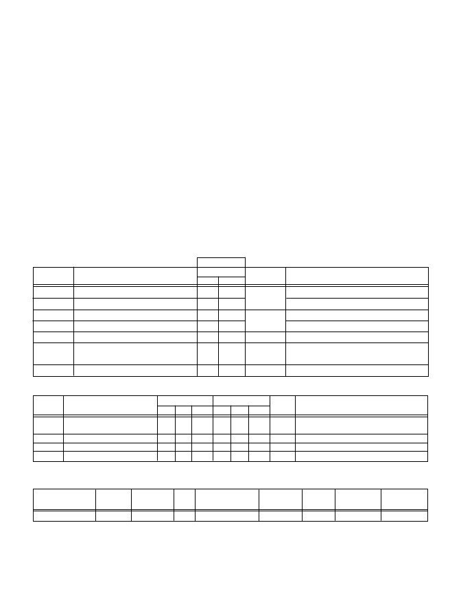
Table 2. High Dose Rate
10
11
Rads (Si)/sec 10
12
Rads (Si)/sec
Min. Typ Max. Min. Typ. Max.
Units
—
—
320
—
Parameter
Drain-to-Source Voltage
Test Conditions
VDSS
—
320
V
Applied drain-to-source voltage
during gamma-dot
Peak radiation induced photo-current
A/μsec Rate of rise of photo-current
μH
Circuit inductance required to limit di/dt
IPP
di/dt
L1
—
—
20
—
—
—
—
—
—
—
—
137
—
—
—
—
—
—
A
Table 3. Single Event Effects
LET (Si)
(MeV/mg/cm
2
)
28
Fluence
(ions/cm
2
)
1 x 10
5
Range
(
μ
m)
~35
V
DS
Bias
(V)
320
V
GS
Bias
(V)
-5
Parameter
Typ.
Units
Ion
BVDSS
400
V
Ni
Radiation Performance of Rad Hard HEXFETs
International Rectifier Radiation Hardened HEX-
FETs are tested to verify their hardness capability.
The hardness assurance program at International
Rectifier uses two radiation environments.
IRHF7310SE Device
Radiation Characteristics
Every manufacturing lot is tested in a low dose rate
(total dose) environment per MlL-STD-750, test
method 1019. International Rectifier has imposed a
standard gate voltage of 12 volts per note 6 and a
V
DSS
bias condition equal to 80% of the device
rated voltage per note 7. Pre- and post-radiation
limits of the devices irradiated to 1 x 10
5
Rads (Si)
are identical and are presented in Table 1. The val-
ues in Table 1 will be met for either of the two low
dose rate test circuits that are used.
Both pre- and post-radiation performance are tested
and specified using the same drive circuitry and test
conditions in order to provide a direct comparison. It
should be noted that at a radiation level of 1 x 10
5
Rads (Si), no change in limits are specified in DC
parameters.
High dose rate testing may be done on a special
request basis, using a dose rate up to 1 x 10
12
Rads
(Si)/Sec.
International Rectifier radiation hardened HEXFETs
have been characterized in neutron and heavy ion
Single Event Effects (SEE) environments. Single
Event Effects characterization is shown in Table 3.
Table 1. Low Dose Rate
Parameter
IRHF7310SE
100K Rads (Si)
min.
400
2.5
—
—
—
—
Units
Test Conditions
max.
—
4.5
100
-100
50
4.5
BV
DSS
V
GS(th)
I
GSS
I
GSS
I
DSS
R
DS(on)1
Drain-to-Source Breakdown Voltage
Gate Threshold Voltage
Gate-to-Source Leakage Forward
Gate-to-Source Leakage Reverse
Zero Gate Voltage Drain Current
Static Drain-to-Source
On-State Resistance One
Diode Forward Voltage
V
V
GS
= 0V, I
D
= 1.0 mA
V
GS
= V
DS
, I
D
= 1.0 mA
V
GS
= 20V
V
GS
= -20V
V
DS
= 0.8 x Max Rating, V
GS
= 0V
V
GS
= 12V, I
D
= 0.7A
nA
μ
A
V
SD
—
1.4
V
TC = 25°C, IS = 1.15A,V
GS
= 0V
相關(guān)PDF資料 |
PDF描述 |
|---|---|
| IRHF7330SE | 400V 100kRad Hi-Rel Single N-Channel SEE Hardened MOSFET in a TO-205AF package |
| IRHF7430SE | 500V 100kRad Hi-Rel Single N-Channel SEE Hardened MOSFET in a TO-205AF package |
| IRHF7310SE | N-Channel Single Event Effect (SEE) Rad Hard HEXFET Transistor(N 溝道 單事件效應(yīng) Rad Hard HEXFET技術(shù)晶體管) |
| IRHF9230 | -200V 100kRad Hi-Rel Single P-Channel TID Hardened MOSFET in a TO-205AF package |
| IRHF93230 | -200V 300kRad Hi-Rel Single P-Channel TID Hardened MOSFET in a TO-205AF package |
相關(guān)代理商/技術(shù)參數(shù) |
參數(shù)描述 |
|---|---|
| IRHF7310SE | 制造商:IRF 制造商全稱:International Rectifier 功能描述:TRANSISTOR N-CHANNEL(BVdss=400V, Rds(on)=4.5ohm, Id=1.15A) |
| IRHF7330SE | 制造商:International Rectifier 功能描述:400V, 2.6A, 1.6 OHM23W - Rail/Tube |
| IRHF7330SESCS | 制造商:International Rectifier 功能描述:HIREL, HEXFET RHD - Bulk |
| IRHF7330SESCV | 制造商:International Rectifier 功能描述:HIREL, HEXFET RHD - Bulk |
| IRHF7430SE | 制造商:International Rectifier 功能描述:HEXFET, HIREL, RAD HARD,G4 - Bulk |
發(fā)布緊急采購(gòu),3分鐘左右您將得到回復(fù)。