- 您現(xiàn)在的位置:買賣IC網(wǎng) > PDF目錄360957 > IRHF7310 PDF資料下載
參數(shù)資料
| 型號: | IRHF7310 |
| 文件頁數(shù): | 2/4頁 |
| 文件大?。?/td> | 36K |
| 代理商: | IRHF7310 |
Thermal Resistance
Parameter
Junction-to-Case
Min. Typ. Max. Units
—
—
Test Conditions
RthJC
8.3
K/W
RthJA
Junction-to-Ambient
—
—
175
Source-Drain Diode Ratings and Characteristics
Parameter
IS
Continuous Source Current (Body Diode)
ISM
Pulse Source Current (Body Diode)
Min. Typ. Max. Units
—
—
—
—
Test Conditions
1.15
4.6
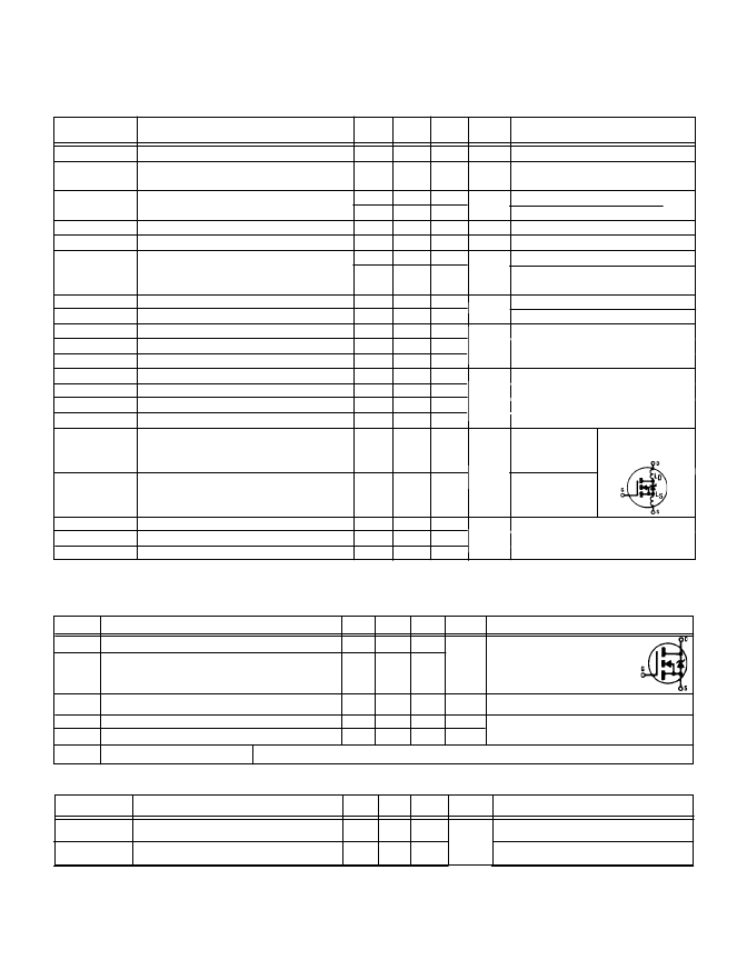
Modified MOSFET symbol showing the
integral reverse p-n junction rectifier.
VSD
trr
QRR
ton
Diode Forward Voltage
Reverse Recovery Time
Reverse Recovery Charge
—
—
—
—
—
—
1.4
540
4.5
V
ns
μ
C
T
j
= 25°C, IS = 1.15A, VGS = 0V
Tj = 25°C, IF = 1.15A, di/dt
≤
100A/
μ
s
VDD
≤
50V
Forward Turn-On Time
Intrinsic turn-on time is negligible. Turn-on speed is substantially controlled by LS + LD.
Electrical Characteristics
@ Tj = 25°C (Unless Otherwise Specified)
Parameter
Drain-to-Source Breakdown Voltage
Temperature Coefficient of Breakdown
Voltage
Static Drain-to-Source
On-State Resistance
Gate Threshold Voltage
Forward Transconductance
Zero Gate Voltage Drain Current
Min.
400
—
Typ. Max. Units
—
—
0.37
—
Test Conditions
VGS = 0V, ID = 1.0 mA
Reference to 25°C, ID = 1.0 mA
BVDSS
BVDSS/
TJ
V
V/°C
RDS(on)
—
—
2.5
0.2
—
—
—
—
—
—
—
—
4.5
5.2
4.5
—
50
250
VGS = 12V, ID = 0.7A
VGS = 12V, ID = 1.15A
VDS = VGS, ID = 1.0 mA
VDS > 15V, IDS = 0.7A
VDS = 0.8 x Max Rating,VGS = 0V
VDS = 0.8 x Max Rating
VGS = 0V, TJ = 125°C
VGS = 20V
VGS = -20V
VGS =12V, ID = 1.15A
VDS = Max. Rating x 0.5
V
VGS(th)
gfs
IDSS
S (
)
IGSS
IGSS
Qg
Qgs
Qgd
td(on)
tr
td(off)
tf
LD
Gate-to-Source Leakage Forward
Gate-to-Source Leakage Reverse
Total Gate Charge
Gate-to-Source Charge
Gate-to-Drain (“Miller”) Charge
Turn-On Delay Time
Rise Time
Turn-Off Delay Time
Fall Time
Internal Drain Inductance
—
—
—
—
—
—
—
—
—
—
—
—
—
—
—
—
—
—
—
5.0
100
-100
10
3
6
15
20
35
30
—
VDD = 200V, ID = 1.15A,
RG = 7.5
LS
Internal Source Inductance
—
15
—
Ciss
Coss
Crss
Input Capacitance
Output Capacitance
Reverse Transfer Capacitance
—
—
—
215
65
—
—
—
—
VGS = 0V, VDS = 25V
f = 1.0 MHz
IRHF7310SE Device
Pre-Radiation
μ
A
nC
pF
nH
ns
Measured from the
drain lead, 6mm (0.25
in.) from package to
center of die.
Measured from the
source lead, 6mm
(0.25 in.) from package
to source bonding pad.
Modified MOSFET
symbol showing the
internal inductances.
nA
A
相關(guān)PDF資料 |
PDF描述 |
|---|---|
| IRHF7330SE | 400V 100kRad Hi-Rel Single N-Channel SEE Hardened MOSFET in a TO-205AF package |
| IRHF7430SE | 500V 100kRad Hi-Rel Single N-Channel SEE Hardened MOSFET in a TO-205AF package |
| IRHF7310SE | N-Channel Single Event Effect (SEE) Rad Hard HEXFET Transistor(N 溝道 單事件效應(yīng) Rad Hard HEXFET技術(shù)晶體管) |
| IRHF9230 | -200V 100kRad Hi-Rel Single P-Channel TID Hardened MOSFET in a TO-205AF package |
| IRHF93230 | -200V 300kRad Hi-Rel Single P-Channel TID Hardened MOSFET in a TO-205AF package |
相關(guān)代理商/技術(shù)參數(shù) |
參數(shù)描述 |
|---|---|
| IRHF7310SE | 制造商:IRF 制造商全稱:International Rectifier 功能描述:TRANSISTOR N-CHANNEL(BVdss=400V, Rds(on)=4.5ohm, Id=1.15A) |
| IRHF7330SE | 制造商:International Rectifier 功能描述:400V, 2.6A, 1.6 OHM23W - Rail/Tube |
| IRHF7330SESCS | 制造商:International Rectifier 功能描述:HIREL, HEXFET RHD - Bulk |
| IRHF7330SESCV | 制造商:International Rectifier 功能描述:HIREL, HEXFET RHD - Bulk |
| IRHF7430SE | 制造商:International Rectifier 功能描述:HEXFET, HIREL, RAD HARD,G4 - Bulk |
發(fā)布緊急采購,3分鐘左右您將得到回復(fù)。