- 您現(xiàn)在的位置:買賣IC網(wǎng) > PDF目錄360867 > INTRO_TO_TRANSISTOR PDF資料下載
參數(shù)資料
| 型號: | INTRO_TO_TRANSISTOR |
| 文件頁數(shù): | 12/13頁 |
| 文件大?。?/td> | 404K |
| 代理商: | INTRO_TO_TRANSISTOR |

Symbol
V
CBO
V
CEO
V
EBO
I
C
I
B
P
C
Tj
Tstg
I
CBO
I
EBO
V
(BR)CEO
h
FE
V
CE
(sat)
V
BE
(sat)
V
FEC
f
T
Cob
Item
Collector-Base Voltage
Collector-Emitter Voltage
Emitter-Base Voltage
Collector Current
Base Current
Collector Power Dissipation
Operating Junction Temperature
Storage Temperature
Collector Cutoff Current
Emitter Cutoff Current
Collector-Emitter Saturation Voltage
DC Current Gain
Collector-Emitter Saturation Voltage
Base-Emitter Saturation Voltage
Emitter-Collector Diode Forward Voltage
Cut-off Frequency
Collector Junction capacitance
Definition
DC Voltage between Collector and Base when Emitter is open
Voltage between Collector and Emitter when Base is open and voltage is reversely applied to Collector junction
DC voltage between Emitter and Base when Collector is open
DC current passing through Collector electrode
DC current passing through Base electrode
Power consumed at Collector junction
Maximum allowable temperature value at absolute maximum ratings
Maximum allowable range of ambient temperature at non-operation
Collector current when Emitter is open and a specified reverse voltage is applied between Collector and Base
Emitter current when Collector is open and a specified reverse voltage is applied between Emitter and Base
Breakdown voltage between Collector and Emitter when Base is open
Ratio of DC output current and DC input current at a specified voltage and current (Emitter common)
DC voltage between Collector and Emitter under specified saturation conditions
DC voltage between Base and Emitter under specified saturation conditions
Diode forward voltage between Emitter and Collector when Base is open
Frequency at the specified voltage and current where h
FE
is 1 (0dB)
Junction capacitance between collector and Base at a specified voltage and frequency
I
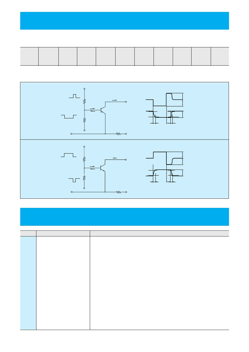
Typical Switching Characteristics
(Common Emitter)
10
I
Switching Characteristics Test Circuit/Measurement Wave Forms
V
CC
(V)
R
L
(
) (A)
I
C
V
B2
(V)
V
BB1
(V)
V
BB2
(V)
I
B1
(A)
I
B2
(A) (
μ
s) (
μ
s) (
μ
s)
t
r
t
stg
t
f
20
μ
s
+
V
BB2
–
V
BB1
R
2
R
1
–
V
CC
0
D.U.T
I
B2
I
C
R
L
I
B1
50
μ
s
0
0
GND
0.9I
C
I
B
I
B
I
C
ton
0
Base
Current
Collector
Current0.1I
C
tstg tf
0
0
20
μ
s
+
V
BB1
–
V
BB2
R
1
R
2
V
CC
0.9I
C
I
B
I
B
I
C
ton
0
0
D.U.T
I
B1
I
C
R
L
I
B2
50
μ
s
0
0
GND
0.1I
C
tstg tf
0
0
Base
Current
Collector
Current
Symbols
NPN
PNP
Switching Characteristics
Ta=25°C unless otherwise specified.
相關(guān)PDF資料 |
PDF描述 |
|---|---|
| INTRUMENT | For EM60000 series |
| IO100VXI | |
| IO110VXI | |
| IO120VXI | |
| IO130VXI | |
相關(guān)代理商/技術(shù)參數(shù) |
參數(shù)描述 |
|---|---|
| INTROVAC XS | 制造商:ABIKO 功能描述:Bulk |
| INTRUMENT | 制造商:未知廠家 制造商全稱:未知廠家 功能描述:For EM60000 series |
| INT-SIGEL | 制造商:Pan Pacific 功能描述: |
| INT-SLVGEL | 制造商:Pan Pacific 功能描述: |
| INTTEST2S3P | 制造商:Panasonic Industrial Devices 功能描述: |
發(fā)布緊急采購,3分鐘左右您將得到回復(fù)。