- 您現(xiàn)在的位置:買賣IC網(wǎng) > PDF目錄67720 > IMIFS782BZBT (CYPRESS SEMICONDUCTOR CORP) 82 MHz, OTHER CLOCK GENERATOR, PDSO8 PDF資料下載
參數(shù)資料
| 型號: | IMIFS782BZBT |
| 廠商: | CYPRESS SEMICONDUCTOR CORP |
| 元件分類: | 時鐘產(chǎn)生/分配 |
| 英文描述: | 82 MHz, OTHER CLOCK GENERATOR, PDSO8 |
| 封裝: | 0.150 INCH, MS-012, SOIC-8 |
| 文件頁數(shù): | 11/12頁 |
| 文件大小: | 246K |
| 代理商: | IMIFS782BZBT |
FS781/82/84
Document #: 38-07029 Rev. *F
Page 8 of 12
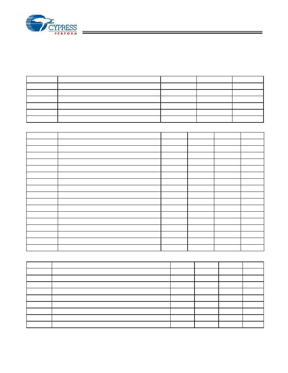
Absolute Maximum Ratings[6]
This device contains circuitry to protect the input against
damage due to high static voltages or electric fields; however,
precautions should be taken to avoid application of any
voltage higher than the absolute maximum rated voltages to
this circuit. For proper operation, VIN and VOUT should be
constrained to the range, VSS < (VIN or VOUT) < VDD. All digital
inputs are tied high or low internally. Refers to electrical speci-
fications for operating supply range.
Table 5. Absolute Maximum Ratings
Parameter
Description
Min.
Max.
Unit
VDD
Operating Voltage
3.0
6.0
VDC
VIRvss
Input, relative to VSS
–0.3
VDD + 0.3
VDC
VORvss
Output, relative to VSS
–0.3
VDD + 0.3
VDC
TOP
Temperature, Operating
0
+70
°C
TST
Temperature, Storage
–65
+150
°C
TJ
Temperature, Junction
–
+125
°C
Table 6. DC Electrical Characteristics VDD = 3.3V and 5.0V ±10%, XIN = 48 MHz, TA = 0°C to 70°C
Parameter
Description
Min.
Typ.
Max.
Unit
VIL
Input Low Voltage
–
0.3 * VDD
VDC
VIH
Input High Voltage
0.7 * VDD
VDC
IIL
Input Low Current
100
A
IIH
Input High Current
100
A
VOL
Output Low Voltage IOL= 10 mA, VDD = 5V
0.4
VDC
VOH
Output High Voltage IOH = 10 mA, VDD = 5V
VDD – 1.0
VDC
VOL
Output Low Voltage IOL= 6 mA, VDD = 3.3V
0.4
VDC
VOH
Output High Voltage IOH = 5 mA, VDD = 3.3V
2.4
VDC
Rpd
Resistor, Pull-down (Pin 7)
60K
125K
200K
Rpu
Resistor, Pull-up (Pin 3)
60K
125K
200K
Cxin
Input Capacitance (Pin 1)
8
pF
Cxout
Output Capacitance (Pin 2)
10
pF
ICC
5V Dynamic Supply Current (CL = No Load)
38
mA
ICC
3.3V Dynamic Supply Current (CL = No Load)
20
mA
ISC
Short Circuit Current (FSOUT)
25
mA
BW
BW% Variations, 3.30V[7]
–20
0
+20
%
BW
BW% Variations, 5.00V[7]
–30
0
+30
%
Table 7. Timing Electrical Characteristics VDD = 3.3V and 5.0V ±10%, TA = 0°C to 70°C, CL = 15 pF, XIN = 48 MHz
Parameter
Description
Min.
Typ.
Max.
Unit
tTLH
Output Rise Time Measured at 10%–90% @ 5 VDC
1.8
2.2
2.7
ns
tTHL
Output Fall Time Measured at 10%–90% @ 5 VDC
1.5
2.0
2.5
ns
tTLH
Output Rise Time Measured at 0.8V–2.0V @ 5 VDC
0.5
0.65
0.8
ns
tTHL
Output Fall Time Measured at 0.8V–2.0 V @ 5 VDC
0.5
0.65
0.8
ns
tTLH
Output Rise Time Measured at 10%–90% @ 3.3 VDC
2.1
2.65
3.2
ns
tTHL
Output Fall Time Measured at 10%–90% @ 3.3 VDC
1.7
2.1
2.6
ns
tTLH
Output Rise Time Measured at 0.8V–2.0V @ 3.3 VDC
0.7
0.95
1.2
ns
tTHL
Output Fall Time Measured at 0.8V–2.0 V @ 3.3 VDC
0.6
0.85
1.1
ns
TsymF1
Output Duty Cycle
45
50
55
%
Notes:
6. Single Power Supply: The Voltage on any input or /O pin cannot exceed the power pin during power-up.
7. Percentage variations from the bandwidth % values given in Table 2 and Table 3.
相關(guān)PDF資料 |
PDF描述 |
|---|---|
| IMIFS784BZBT | 82 MHz, OTHER CLOCK GENERATOR, PDSO8 |
| IMISC643AYB | PROC SPECIFIC CLOCK GENERATOR, PDSO48 |
| IMISC670DYB | PROC SPECIFIC CLOCK GENERATOR, PDSO48 |
| IMISG522BXB | OTHER CLOCK GENERATOR, PDSO16 |
| IMISG522BX | 120 MHz, OTHER CLOCK GENERATOR, PDSO16 |
相關(guān)代理商/技術(shù)參數(shù) |
參數(shù)描述 |
|---|---|
| IMIFS784BT | 制造商:CYPRESS 制造商全稱:Cypress Semiconductor 功能描述:Low EMI Spectrum Spread Clock |
| IMIFS784BTT | 制造商:CYPRESS 制造商全稱:Cypress Semiconductor 功能描述:Low EMI Spectrum Spread Clock |
| IMIFS784BZB | 制造商:Rochester Electronics LLC 功能描述:PREMIS EMI REDUCTION SSCG - Bulk |
| IMIFS784BZBT | 制造商:CYPRESS 制造商全稱:Cypress Semiconductor 功能描述:Low EMI Spectrum Spread Clock |
| IMIFS786BZB | 制造商:Cypress Semiconductor 功能描述: |
發(fā)布緊急采購,3分鐘左右您將得到回復(fù)。