- 您現(xiàn)在的位置:買賣IC網(wǎng) > PDF目錄383103 > IH5352CBP (INTERSIL CORP) Quad SPST, CMOS RF/Video Switch PDF資料下載
參數(shù)資料
| 型號(hào): | IH5352CBP |
| 廠商: | INTERSIL CORP |
| 元件分類: | 運(yùn)動(dòng)控制電子 |
| 英文描述: | Quad SPST, CMOS RF/Video Switch |
| 中文描述: | QUAD 1-CHANNEL, SGL POLE SGL THROW SWITCH, PDSO20 |
| 封裝: | SOIC-20 |
| 文件頁(yè)數(shù): | 5/8頁(yè) |
| 文件大小: | 118K |
| 代理商: | IH5352CBP |
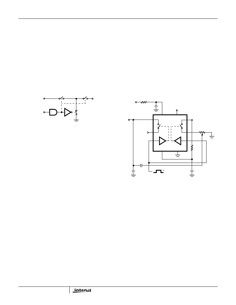
5
Detailed Description
Figure 5 shows the internal circuit of one channel of the
IH5352. Here, a shunt switch is closed, and the two series
switches are open when the video switch channel is open or
off. This provides much better isolation between the input
and output terminals than a simple series switch does,
especially at high frequencies. The result is excellent off-
isolation in the Video and RF frequency ranges when
compared to conventional analog switches.
The control input level shifting circuitry is very similar to that
of the IH5140 series of Analog Switches, and gives very high
speed, guaranteed “Break-Before-Make” action, low static
power consumption and TTL compatibility.
Typical Applications
Charge Compensation Techniques
Charge injection results from the signals out of the level
translation circuit being coupled through the gate-channel
and gate-source/drain capacitances to the switch inputs and
outputs. This feedthrough is particularly troublesome in
Sample-and-Hold or Track-and-Hold applications, as it
causes a Sample (Track) to Hold offset. The IH5352 has a
typical injected charge of 30pC-50pC (corresponding to
30mV-50mV on a 1000pF capacitor), at V
S-D
of about 0V.
This Sample (Track) to Hold offset can be compensated by
bringing in a signal equal in magnitude but of the opposite
polarity. The circuit of Figure 6 accomplishes this charge
injection compensation by using one side of the device as a
S & H (T & H) switch, and the other side as a generator of a
compensating signal. The 1k
potentiometer allows the user
to adjust the net injected charge to exactly zero for any
analog voltage in the -5V to +5V range.
Since individual parts are very consistent in their charge
injection, it is possible to replace the potentiometer with a
pair of fixed resistors, and achieve less than 5mV error for
all devices without adjustment.
generate the required inversion, is shown in Figure 7. The
capacitorneedstobeincreased,andbecomestheonlymethod
of adjustment. A fixed value of 22pF is good for analog values
referred to ground, while 35pF is optimum for AC coupled
signals referred to -5V as shown in the figure. The choice of -5V
is based on the virtual disappearance at this analog level of the
transient component of switching charge injection. This
combination will lead to a virtually “glitch-free” switch.
SWITCH
SOURCE
(VIDEO INPUT)
SWITCH
DRAIN
(VIDEO
OUTPUT)
LOGIC
DRIVER
TRANSLATOR
CONTROL
INPUT
NOTE: 1 channel of 4 shown.
FIGURE 5. INTERNAL SWITCH CONFIGURATION
SHUNT
SWITCH
S
1
IN
1
D
1
5V
GND
V+
V
L
S
2
IN
2
D
2
V-
ANALOG
INPUT
75
75
-15V
1k
CERMET
NOT WIRE
WOUND (NOTE)
10pF
1
μ
F
15V
TTL IN (STROBE)
+3V
0V
V
OUT
1000pF
C
HOLD
NOTE: Adjust pot for 0mV
P-P
step at V
OUT
with no analog (AC)
signal present.
FIGURE 6. CHARGE INJECTION COMPENSATION
1
μ
F
IH5352
相關(guān)PDF資料 |
PDF描述 |
|---|---|
| IH5352CPE | Quad SPST, CMOS RF/Video Switch |
| IHD 215 | IGBT And Power-MOSFET(IGBT和功率MOSFET) |
| IHD 280 | IGBT And Power-MOSFET(IGBT和功率MOSFET) |
| IHD 680 | IGBT And Power-MOSFET(IGBT和功率MOSFET) |
| IHP10T120 | Low Loss DuoPack : IGBT in Trench and Fieldstop technology with soft, fast recovery anti-parallel EmCon HE diode |
相關(guān)代理商/技術(shù)參數(shù) |
參數(shù)描述 |
|---|---|
| IH5352CPD | 制造商:未知廠家 制造商全稱:未知廠家 功能描述:Interface IC |
| IH5352CPE | 功能描述:視頻開(kāi)關(guān) IC RoHS:否 制造商:Texas Instruments 開(kāi)關(guān)數(shù)量:4 開(kāi)啟電阻(最大值):12 Ohms 傳播延遲時(shí)間: 開(kāi)啟時(shí)間(最大值): 關(guān)閉時(shí)間(最大值): 最大工作溫度:+ 85 C 最小工作溫度:- 40 C 封裝 / 箱體:WQFN-42 封裝:Reel |
| IH5352CPE WAF | 制造商:Intersil Corporation 功能描述: |
| IH5352CPE+ | 功能描述:視頻開(kāi)關(guān) IC Quad RF/Video Switch RoHS:否 制造商:Texas Instruments 開(kāi)關(guān)數(shù)量:4 開(kāi)啟電阻(最大值):12 Ohms 傳播延遲時(shí)間: 開(kāi)啟時(shí)間(最大值): 關(guān)閉時(shí)間(最大值): 最大工作溫度:+ 85 C 最小工作溫度:- 40 C 封裝 / 箱體:WQFN-42 封裝:Reel |
| IH5352CPE-2 | 制造商:未知廠家 制造商全稱:未知廠家 功能描述:SPST Analog Switch |
發(fā)布緊急采購(gòu),3分鐘左右您將得到回復(fù)。