- 您現(xiàn)在的位置:買(mǎi)賣(mài)IC網(wǎng) > PDF目錄377486 > IDT7MB4045S15Z (Integrated Device Technology, Inc.) 256K x 32 CMOS STATIC RAM MODULE PDF資料下載
參數(shù)資料
| 型號(hào): | IDT7MB4045S15Z |
| 廠商: | Integrated Device Technology, Inc. |
| 英文描述: | 256K x 32 CMOS STATIC RAM MODULE |
| 中文描述: | 256K × 32的CMOS靜態(tài)RAM模塊 |
| 文件頁(yè)數(shù): | 1/8頁(yè) |
| 文件大?。?/td> | 96K |
| 代理商: | IDT7MB4045S15Z |
2703 drw 01
PD
0
PD
1
31
29
9
11
13
15
17
19
21
23
25
27
1
3
5
7
33
35
37
39
63
61
41
43
45
47
49
51
53
55
57
59
– GND
– GND
32
30
28
8
10
12
14
16
18
20
22
24
26
2
4
6
34
36
38
40
64
62
42
44
46
48
50
52
54
56
58
60
GND
I/O
16
I/O
17
I/O
18
I/O
19
A
10
A
11
A
12
A
13
I/O
20
I/O
21
I/O
22
I/O
23
GND
CS
3
A
16
I/O
0
I/O
1
I/O
2
I/O
3
V
CC
A
7
A
8
A
9
I/O
4
I/O
5
I/O
6
I/O
7
WE
A
14
CS
1
PD
0
CS
4
A
17
OE
I/O
24
I/O
25
I/O
26
I/O
27
A
3
A
4
A
5
V
CC
A
6
I/O
28
I/O
29
I/O
30
I/O
31
PD
1
I/O
8
I/O
9
I/O
10
I/O
11
A
0
A
1
A
2
I/O
12
I/O
13
I/O
14
I/O
15
GND
A
15
GND
CS
2
FEATURES:
High density 1 megabyte static RAM module
(IDT7MP4145 upgradeable to 4 megabyte, IDT7MP4120)
Low profile 64 pin ZIP (Zig-zag In-line vertical Package)
or 64 pin SIMM (Single In-line Memory Module) for
IDT7MP4045 and 72 pin SIMM (Single In-line Memory
Module) for IDT7MP4145
Very fast access time: 15ns (max.)
Surface mounted plastic components on an epoxy
laminate (FR-4) substrate
Single 5V (
±
10%) power supply
Multiple GND pins and decoupling capacitors for maxi-
mum noise immunity
Inputs/outputs directly TTL-compatible
PIN NAMES
I/O
0
–
31
A
0
–
17
CS
1–4
Data Inputs/Outputs
Addresses
Chip Selects
Write Enable
Output Enable
Depth Identification
Power
Ground
No Connect
WE
OE
PD
0–1
V
CC
GND
NC
2703 tbl 01
Integrated Device Technology, Inc.
COMMERCIAL TEMPERATURE RANGE
SEPTEMBER 1996
1996 Integrated Device Technology, Inc.
DSC-2703/7
1
The IDT logo is a registered trademark of Integrated Device Technology Inc.
NOTE:
1. Pins 2 and 3 (PD
0
and PD
1
) are read by the user to determine the density
of the module. If PD
0
reads GND and PD
1
reads GND, then the module
has a 256K depth.
DESCRIPTION:
The IDT7MP4045/4145 is a 256K x 32 static RAM module
constructed on an epoxy laminate (FR-4) substrate using 8
256K x 4 static RAMs in plastic SOJ packages. Availability of
four chip select lines (one for each group of two RAMs)
provides byte access. The IDT7MP4045 is available with
access time as fast as 10ns with minimal power consumption.
The IDT7MP4045 is packaged in a 64 pin FR-4 ZIP (Zig-
zag In-line vertical Package)or a 64 pin SIMM (Single In-line
Memory Module) where as the 7MP4145 is packaged in a 72
pin SIMM (Single In-line Memory Module). The 4045 ZIP
configuration allows 64 pins to be placed on a package 3.65
inches long and 0.365 inches wide. The 7MP4045 ZIP is only
0.585 inches high, this low profile package is ideal for systems
with minimum board spacing while the SIMM configuration
allows use of edge mounted sockets to secure the module.
All inputs and outputs of the IDT7MP4045/4145 are TTL-
compatible and operate from a single 5V supply. Full asyn-
chronous circuitry requires no clocks or refresh for operation
and provides equal access and cycle times for ease of use.
Identification pins are provided for applications in which
different density versions of the module are used. In this way,
the target system can read the respective levels of PD
pins
to
determine a 256K depth.
The contact pins are plated with 100 micro-inches of nickel
covered by 30 micro-inches minimum of selective gold.
PIN CONFIGURATION – 7MP4045
(1)
ZIP, SIMM
TOP VIEW
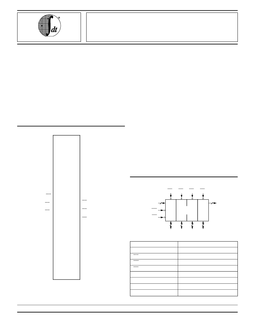
FUNCTIONAL BLOCK DIAGRAM
OE
WE
2703 drw 02
8
18
256K x 32
RAM
8
8
8
2
CS
1
CS
2
CS
3
CS
4
ADDRESS
I/O
0-31
PD
IDT7MP4045
IDT7MP4145
256K x 32
CMOS STATIC RAM MODULE
15.2
相關(guān)PDF資料 |
PDF描述 |
|---|---|
| IDT7MB4045S20M | 256K x 32 CMOS STATIC RAM MODULE |
| IDT7MB4045S20Z | 256K x 32 CMOS STATIC RAM MODULE |
| IDT7MP4045 | 256K x 32 CMOS STATIC RAM MODULE |
| IDT7MPV6253S15M | 256KB AND 512KB SECONDARY CACHE MODULES FOR THE PowerPCO |
| IDT7MPV6253S66M | 256KB AND 512KB SECONDARY CACHE MODULES FOR THE PowerPCO |
相關(guān)代理商/技術(shù)參數(shù) |
參數(shù)描述 |
|---|---|
| IDT7MP4036S25Z | 制造商:Integrated Device Technology Inc 功能描述: |
| IDT80ALVCH16823PA | 制造商:IDT 制造商全稱(chēng):Integrated Device Technology 功能描述:3.3V CMOS 18-BIT BUS-INTERFACE FLIPFLOP WITH 3-STATE OUTPUTS AND BUS-HOLD |
| IDT80HCPS1432CHM | 制造商:Integrated Device Technology Inc 功能描述:IC RIO SWITCH GEN2 576FCBGA |
| IDT80HCPS1432CHMI | 制造商:Integrated Device Technology Inc 功能描述:IC RIO SWITCH GEN2 576FCBGA |
| IDT80HCPS1432CRM | 制造商:Integrated Device Technology Inc 功能描述:IC RIO SWITCH GEN2 576FCBGA |
發(fā)布緊急采購(gòu),3分鐘左右您將得到回復(fù)。