- 您現(xiàn)在的位置:買賣IC網(wǎng) > PDF目錄377485 > IDT7M1003S50C (INTEGRATED DEVICE TECHNOLOGY INC) 128K x 8 64K x 8 CMOS DUAL-PORT STATIC RAM MODULE PDF資料下載
參數(shù)資料
| 型號(hào): | IDT7M1003S50C |
| 廠商: | INTEGRATED DEVICE TECHNOLOGY INC |
| 元件分類: | DRAM |
| 英文描述: | 128K x 8 64K x 8 CMOS DUAL-PORT STATIC RAM MODULE |
| 中文描述: | 64K X 8 MULTI-PORT DEVICE SRAM MODULE, 50 ns, DMA64 |
| 文件頁(yè)數(shù): | 7/11頁(yè) |
| 文件大?。?/td> | 171K |
| 代理商: | IDT7M1003S50C |
IDT7M1001/1003
128K/64K x 8 CMOS DUAL-PORT STATIC RAM MODULE
MILITARY AND COMMERCIAL TEMPERATURE RANGES
7.5
7
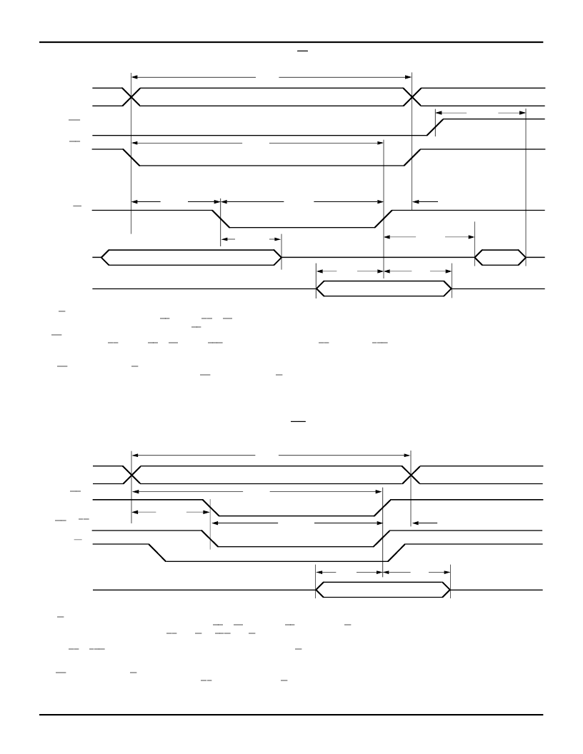
TIMING WAVEFORM OF WRITE CYCLE NO. 1 (R/
W
CONTROLLED TIMING)
(1,3,5,8)
ADDRESS
OE
CS
t
WC
t
OHZ(9)
t
AW
R/W
t
WP(2)
t
AS
t
WHZ(9)
DATA
OUT
DATA
IN
(4)
(4)
t
OW(9)
t
DW
t
DH
t
WR(7)
DATA VALID
(6)
2804 drw 08
TIMING WAVEFORM OF WRITE CYCLE NO. 2 (
CS
CONTROLLED TIMING)
(1,3,5,8)
NOTES:
1. R/
W
must be HIGH during all address transitions.
2. A write occurs during the overlap (t
WP
) of a LOW
UB
or
LB
and a LOW
CS
and a LOW R/
W
for memory array writing cycle.
3. t
WR
is measured from the earlier of
CS
or R/
W
(or
SEM
or R/
W
) going HIGH to the end of write cycle.
4. During this period, the I/O pins are in the output state and input signals must not be applied.
5. If the
CS
or
SEM
LOW transition occurs simultaneously with or after the R/
W
LOW transition, the outputs remain in the high-impedance state.
6. Timing depends on which enable signal is asserted last.
7. Timing depends on which enable signal is de-asserted first.
8. If
OE
is LOW during a R/
W
controlled write cycle, the write pulse width must be the larger of t
WP
or (t
WZ
+ t
DW
) to allow the I/O drivers to turn off and data
to be placed on the bus for the required t
DW
. If
OE
is HIGH during an R/
W
controlled write cycle, this requirement does not apply and the write pulse can
be as short as the specified t
WP
.
9. This parameter is guaranteed by design but not tested.
NOTES:
1. R/
W
is HIGH for Read Cycles
2. Device is continuously enabled.
CS
= LOW.
UB
or
LB
= LOW. This waveform cannot be used for semaphore reads.
3. Addresses valid prior to or coincident with
CS
transition low.
4.
OE
= LOW.
5. To access RAM,
CS
= LOW,
UB
or
LB
= LOW,
SEM
= H. To access semaphore,
CS
= HIGH and
SEM
= LOW.
6. Timing depends on which enable signal is asserted last.
7. Timing depends on which enable signal is de-asserted first.
8. If
OE
is LOW during a R/
W
controlled write cycle, the write pulse width must be larger of t
WP
or (t
WZ
+ t
DW
) to allow the I/O drivers to turn off and data to
be placed on the bus for the required tDW. If
OE
is HIGH during a R/
W
controlled write cycle, this requirement does not apply and the write pulse width
be as short as the specified t
WP
.
9. This parameter is guaranteed by design but not tested.
ADDRESS
t
WC
DATA
IN
t
DW
t
DH
DATA VALID
t
AW
R/W
t
WP(2)
t
WR(7)
CS
t
AS(6)
UB
LB
or
2804 drw 09
相關(guān)PDF資料 |
PDF描述 |
|---|---|
| IDT7M1003S50CB | 128K x 8 64K x 8 CMOS DUAL-PORT STATIC RAM MODULE |
| IDT7M1002 | 16K x 32 CMOS DUAL-PORT STATIC RAM MODULE |
| IDT7M1002S30G | 16K x 32 CMOS DUAL-PORT STATIC RAM MODULE |
| IDT7M1002S30GB | 16K x 32 CMOS DUAL-PORT STATIC RAM MODULE |
| IDT7M1002S35G | 16K x 32 CMOS DUAL-PORT STATIC RAM MODULE |
相關(guān)代理商/技術(shù)參數(shù) |
參數(shù)描述 |
|---|---|
| IDT7M134S45C | 制造商:IDT 功能描述:IDT7M134S45C |
| IDT7M135S45C | 制造商:IDT 功能描述:IDT7M135S45C |
| IDT7M464S65C | 制造商:Integrated Device Technology Inc 功能描述:Static RAM Memory Module, 16K x 4, 22 Pin, Ceramic, DIP |
| IDT7M464S85C | 制造商:Integrated Device Technology Inc 功能描述:Static RAM Memory Module, 16K x 4, 22 Pin, Ceramic, DIP |
| IDT7M624S45CB | 制造商:Integrated Device Technology Inc 功能描述: |
發(fā)布緊急采購(gòu),3分鐘左右您將得到回復(fù)。