- 您現(xiàn)在的位置:買賣IC網(wǎng) > PDF目錄4583 > IDT72V51446L6BB8 (IDT, Integrated Device Technology Inc)IC FLOW CTRL MULTI QUEUE 256-BGA PDF資料下載
參數(shù)資料
| 型號: | IDT72V51446L6BB8 |
| 廠商: | IDT, Integrated Device Technology Inc |
| 文件頁數(shù): | 10/57頁 |
| 文件大小: | 0K |
| 描述: | IC FLOW CTRL MULTI QUEUE 256-BGA |
| 標(biāo)準(zhǔn)包裝: | 1,000 |
| 類型: | 多隊(duì)列流量控制 |
| 安裝類型: | 表面貼裝 |
| 封裝/外殼: | 256-BBGA |
| 供應(yīng)商設(shè)備封裝: | 256-BGA(17x17) |
| 包裝: | 帶卷 (TR) |
| 其它名稱: | 72V51446L6BB8 |
第1頁第2頁第3頁第4頁第5頁第6頁第7頁第8頁第9頁當(dāng)前第10頁第11頁第12頁第13頁第14頁第15頁第16頁第17頁第18頁第19頁第20頁第21頁第22頁第23頁第24頁第25頁第26頁第27頁第28頁第29頁第30頁第31頁第32頁第33頁第34頁第35頁第36頁第37頁第38頁第39頁第40頁第41頁第42頁第43頁第44頁第45頁第46頁第47頁第48頁第49頁第50頁第51頁第52頁第53頁第54頁第55頁第56頁第57頁

18
COMMERCIALANDINDUSTRIAL
TEMPERATURERANGES
IDT72V51436/72V51446/72V51456 3.3V, MULTI-QUEUE FLOW-CONTROL DEVICES
(16 QUEUES) 36 BIT WIDE CONFIGURATION 589,824, 1,179,648 and 2,359,296 bits
cycles are required for the device to load its internal setup registers. When a
single multi-queue is used, the completion of device programming is signaled
bythe
SENOoutputofadevicegoingfromHIGHtoLOW.Note,thatSENImust
be held LOW when a device is setup for default programming mode.
When multi-queue devices are connected in expansion mode, the
SENI of
thefirstdeviceinachaincanbeheldLOW.The
SENOofadeviceshouldconnect
to the
SENIofthenextdeviceinthechain.TheSENOofthefinaldeviceisused
to indicate that default programming of all devices is complete. When the final
SENO goes LOW normal operations may begin. Again, all devices will be
programmed with their maximum number of queues and the memory divided
equally between them. Please refer to Figure 8, Default Programming.
READING AND WRITING TO THE IDT MULTI-QUEUE
FLOW CONTROL MANAGER
The IDT72V51436/72V51446/72V51456 multi-queue flow-control de-
vices can be configured in two distinct modes, namely Standard Mode and
Packet Mode.
STANDARD MODE OPERATION (PKT = LOW on Master Reset)
WRITE QUEUE SELECTION AND WRITE OPERATION
(STANDARD MODE)
The IDT72V51436/72V51446/72V51456 multi-queue flow-control de-
vices can be configured up to a maximum of 16 queues into which data can
be written via a common write port using the data inputs (Din), write clock
(WCLK) and write enable (
WEN). The queue to be written is selected by the
address present on the write address bus (WRADD) during a rising edge on
WCLK while write address enable (WADEN) is HIGH. The state of
WENdoes
notimpactthequeueselection.Thequeueselectionisrequires2WCLKcycles.
All subsequent data writes will be to this queue until another queue is selected.
Standard mode operation is defined as individual words will be written to the
device as opposed to Packet Mode where complete packets may be written.
The write port is designed such that 100% bus utilization can be obtained. This
means that data can be written into the device on every WCLK rising edge
including the cycle that a new queue is being addressed.
Changing queues requires a minimum of 2 WCLK cycles on the write port
(see Figure 9, Write Queue Select, Write Operation and Full flag Operation).
WADEN goes high signaling a change of queue (clock cycle “A”). The address
onWRADDatthattimedeterminesthenextqueue.Datapresentedduringthat
cycle (“A”) and the next cycle (“B”), will be written to the active (old) queue,
provided
WEN is active LOW. If WEN is HIGH (inactive) for these two clock
cycles, data will not be written in to the previous queue. The write port discrete
full flag will update to show the full status of the newly selected queue (Q
X) at
this last cycle’s rising edge (“B”). Data present on the data input bus (Din), can
be written into the newly selected queue (Q
X) on the rising edge of WCLK on
the second cycle (“C”) following a change of queue, provided
WEN is LOW
and the new queue is not full. If the newly selected queue is full at the point of
its selection, any writes to that queue will be prevented. Data cannot be written
into a full queue.
Refer to Figure 9, Write Queue Select, Write Operation and Full flag
Operation, Figure 10, Write Operations & First Word Fall Through for timing
diagrams and Figure 11, Full Flag Timing in Expansion Mode for timing
diagrams.
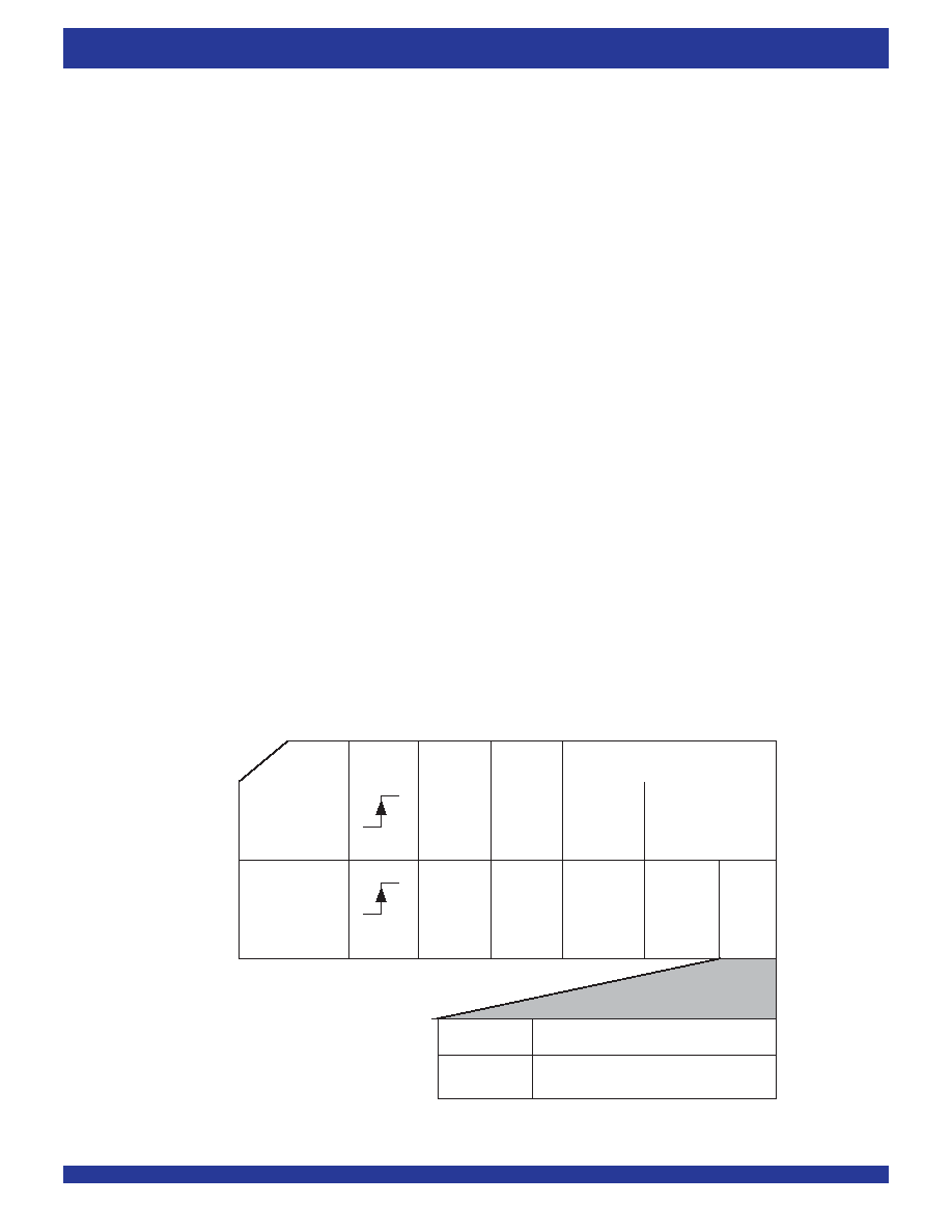
TABLE 1 — WRITE ADDRESS BUS, WRADD[7:0]
Operation WCLK WADEN
FSTR
WRADD[6:0]
Write Queue
Select
10
01
Device Select
(Compared to
ID0,1,2)
Write Queue Address
(4 bits = 16 Queues)
654
3 2
1 0
765 4 3
1
0
Device Select
(Compared to
ID0,1,2)
X X
X
Sector
Address
PAFn Sector
Select
Q0 : Q7
→ PAF0 : PAF7
Sector
Address
Queue Status on
PAFn Bus
0
1
Q8 : Q15
→ PAF0 : PAF7
5935 drw05
2
X
相關(guān)PDF資料 |
PDF描述 |
|---|---|
| IDT72V51443L6BB8 | IC FLOW CTRL MULTI QUEUE 256-BGA |
| LT1020CSW#TR | IC REG LDO ADJ 125MA 16SOIC |
| MIC5259-3.3YML TR | IC REG LDO 3.3V .3A 6-MLF |
| LT1020CSW#TRPBF | IC REG LDO ADJ 125MA 16-SOIC |
| LFECP15E-3FN256C | IC FPGA 15.3KLUTS 195I/O 256-BGA |
相關(guān)代理商/技術(shù)參數(shù) |
參數(shù)描述 |
|---|---|
| IDT72V51446L7-5BB | 功能描述:IC FLOW CTRL MULTI QUEUE 256-BGA RoHS:否 類別:集成電路 (IC) >> 專用 IC 系列:- 產(chǎn)品培訓(xùn)模塊:Lead (SnPb) Finish for COTS Obsolescence Mitigation Program 標(biāo)準(zhǔn)包裝:1 系列:- 類型:調(diào)幀器 應(yīng)用:數(shù)據(jù)傳輸 安裝類型:表面貼裝 封裝/外殼:400-BBGA 供應(yīng)商設(shè)備封裝:400-PBGA(27x27) 包裝:散裝 |
| IDT72V51446L7-5BB8 | 功能描述:IC FLOW CTRL MULTI QUEUE 256-BGA RoHS:否 類別:集成電路 (IC) >> 專用 IC 系列:- 產(chǎn)品培訓(xùn)模塊:Lead (SnPb) Finish for COTS Obsolescence Mitigation Program 標(biāo)準(zhǔn)包裝:1 系列:- 類型:調(diào)幀器 應(yīng)用:數(shù)據(jù)傳輸 安裝類型:表面貼裝 封裝/外殼:400-BBGA 供應(yīng)商設(shè)備封裝:400-PBGA(27x27) 包裝:散裝 |
| IDT72V51446L7-5BBI | 功能描述:IC FLOW CTRL MULTI QUEUE 256-BGA RoHS:否 類別:集成電路 (IC) >> 專用 IC 系列:- 產(chǎn)品培訓(xùn)模塊:Lead (SnPb) Finish for COTS Obsolescence Mitigation Program 標(biāo)準(zhǔn)包裝:1 系列:- 類型:調(diào)幀器 應(yīng)用:數(shù)據(jù)傳輸 安裝類型:表面貼裝 封裝/外殼:400-BBGA 供應(yīng)商設(shè)備封裝:400-PBGA(27x27) 包裝:散裝 |
| IDT72V51453L6BB | 功能描述:IC FLOW CTRL MULTI QUEUE 256-BGA RoHS:否 類別:集成電路 (IC) >> 專用 IC 系列:- 產(chǎn)品培訓(xùn)模塊:Lead (SnPb) Finish for COTS Obsolescence Mitigation Program 標(biāo)準(zhǔn)包裝:1 系列:- 類型:調(diào)幀器 應(yīng)用:數(shù)據(jù)傳輸 安裝類型:表面貼裝 封裝/外殼:400-BBGA 供應(yīng)商設(shè)備封裝:400-PBGA(27x27) 包裝:散裝 |
| IDT72V51453L6BB8 | 功能描述:IC FLOW CTRL MULTI QUEUE 256-BGA RoHS:否 類別:集成電路 (IC) >> 專用 IC 系列:- 產(chǎn)品培訓(xùn)模塊:Lead (SnPb) Finish for COTS Obsolescence Mitigation Program 標(biāo)準(zhǔn)包裝:1 系列:- 類型:調(diào)幀器 應(yīng)用:數(shù)據(jù)傳輸 安裝類型:表面貼裝 封裝/外殼:400-BBGA 供應(yīng)商設(shè)備封裝:400-PBGA(27x27) 包裝:散裝 |
發(fā)布緊急采購,3分鐘左右您將得到回復(fù)。