- 您現(xiàn)在的位置:買賣IC網(wǎng) > PDF目錄377422 > IDT72825LB15BGI (INTEGRATED DEVICE TECHNOLOGY INC) CMOS DUAL SyncFIFO DUAL 256 x 18, DUAL 512 x 18, DUAL 1,024 x 18, DUAL 2,048 x 18, and DUAL 4,096 x 18 PDF資料下載
參數(shù)資料
| 型號: | IDT72825LB15BGI |
| 廠商: | INTEGRATED DEVICE TECHNOLOGY INC |
| 元件分類: | DRAM |
| 英文描述: | CMOS DUAL SyncFIFO DUAL 256 x 18, DUAL 512 x 18, DUAL 1,024 x 18, DUAL 2,048 x 18, and DUAL 4,096 x 18 |
| 中文描述: | 1K X 18 BI-DIRECTIONAL FIFO, 10 ns, PBGA121 |
| 封裝: | 16 X 16 MM, PLASTIC, BGA-121 |
| 文件頁數(shù): | 25/26頁 |
| 文件大?。?/td> | 334K |
| 代理商: | IDT72825LB15BGI |
第1頁第2頁第3頁第4頁第5頁第6頁第7頁第8頁第9頁第10頁第11頁第12頁第13頁第14頁第15頁第16頁第17頁第18頁第19頁第20頁第21頁第22頁第23頁第24頁當(dāng)前第25頁第26頁
25
COMMERCIAL AND INDUSTRIAL
TEMPERATURE RANGES
IDT72805LB/72815LB/72825LB/72835LB/72845LB CMOS Dual SyncFIFO
TM
256 x 18, 512 x 18, 1,024 x 18, 2,048 x 18 and 4,096 x 18
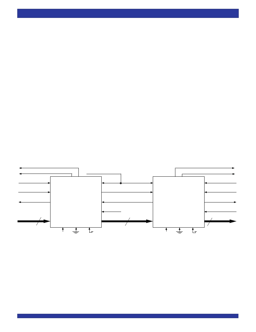
Figure 31. Block Diagram of 512 x 18, 1,024 x 18, 2,048 x 18, 4,096 x 18, 8,192 x 18 Synchronous
FIFO Memory With Programmable Flags used in Depth Expansion Configuration
Dn
INPUT READY
WRITE ENABLE
WRITE CLOCK
WEN
WCLK
IR
DATA IN
RCLK
READ CLOCK
RCLK
REN
OE
OUTPUT ENABLE
OUTPUT READY
Qn
Dn
IR
GND
WEN
WCLK
OR
REN
OE
Qn
READ ENABLE
OR
DATA OUT
TRANSFER CLOCK
3139 drw 31
n
n
n
RXI
HF
72805
72815
72825
72835
72845
WXI
FL
V
CC
GND
(0,1)
72805
72815
72825
72835
72845
RXI
WXI
FL
V
CC
GND
(0,1)
PAF
HF
PAE
DEPTH EXPANSION CONFIGURATION (FWFT MODE)
In FWFT mode, the FIFOs can be connected in series (the data outputs
of one FIFO connected to the data inputs of the next) with no external logic
necessary. The resulting configuration provides a total depth equivalent to
the sumof the depths associated with each single FIFO. Figure 31 shows
a depth expansion using one IDT72805LB/72815LB/72825LB/72835LB/
72845LB devices.
Care should be taken to select FWFT mode during Master Reset for all
FIFOs in the depth expansion configuration. The first word written to an
empty configuration will pass fromone FIFO to the next (“ripple down”) until
it finally appears at the outputs of the last FIFO in the chain–no read
operation is necessary but the RCLK of each FIFO must be free-running.
Each time the data word appears at the outputs of one FIFO, that device’s
OR
line goes LOW, enabling a write to the next FIFO in line.
For an empty expansion configuration, the amount of time it takes for
OR
of the last FIFO in the chain to go LOW (i.e. valid data to appear on the last
FIFO’s outputs) after a word has been written to the first FIFO is the sumof
the delays for each individual FIFO:
(N – 1)*4*transfer clock) + 3*T
RCLK
where N is the number of FIFOs in the expansion and T
RCLK
is the RCLK
period. Note that extra cycles should be added for the possibility that the
t
SKEW1
specification is not met between WCLK and transfer clock, or RCLK
and transfer clock, for the
OR
flag.
The “ripple down” delay is only noticeable for the first word written to an
empty depth expansion configuration. There will be no delay evident for
subsequent words written to the configuration.
The first free location created by reading froma full depth expansion
configuration will “bubble up” fromthe last FIFO to the previous one until it
finally moves into the first FIFO of the chain. Each time a free location is
created in one FIFO of the chain, that FIFO’s
IR
line goes LOW, enabling
the preceding FIFO to write a word to fill it.
For a full expansion configuration, the amount of time it takes for
IR
of the
first FIFO in the chain to go LOW after a word has been read fromthe last
FIFO is the sumof the delays for each individual FIFO:
(N – 1)*3*transfer clock) + 2 T
WCLK
where N is the number of FIFOs in the expansion and T
WCLK
is the WCLK
period. Note that extra cycles should be added for the possibility that the
t
SKEW1
specification is not met between RCLK and transfer clock, or WCLK
and transfer clock, for the
IR
flag.
The Transfer Clock line should be tied to either WCLK or RCLK,
whichever is faster. Both these actions result in data moving, as quickly as
possible, to the end of the chain and free locations to the beginning of the
chain.
相關(guān)PDF資料 |
PDF描述 |
|---|---|
| IDT72825LB15PF | CMOS DUAL SyncFIFO DUAL 256 x 18, DUAL 512 x 18, DUAL 1,024 x 18, DUAL 2,048 x 18, and DUAL 4,096 x 18 |
| IDT72825LB15PFI | CMOS DUAL SyncFIFO DUAL 256 x 18, DUAL 512 x 18, DUAL 1,024 x 18, DUAL 2,048 x 18, and DUAL 4,096 x 18 |
| IDT72825LB20BGI | CMOS DUAL SyncFIFO DUAL 256 x 18, DUAL 512 x 18, DUAL 1,024 x 18, DUAL 2,048 x 18, and DUAL 4,096 x 18 |
| IDT72845LB | Precision Micropower Shunt Voltage Reference 5-SC70 -40 to 85 |
| IDT72845LB10PF | CMOS DUAL SyncFIFO DUAL 256 x 18, DUAL 512 x 18, DUAL 1,024 x 18, DUAL 2,048 x 18, and DUAL 4,096 x 18 |
相關(guān)代理商/技術(shù)參數(shù) |
參數(shù)描述 |
|---|---|
| IDT72825LB15PF | 功能描述:IC FIFO SYNC DL 1024X18 128TQFP RoHS:否 類別:集成電路 (IC) >> 邏輯 - FIFO 系列:7200 標(biāo)準(zhǔn)包裝:90 系列:7200 功能:同步 存儲(chǔ)容量:288K(16K x 18) 數(shù)據(jù)速率:100MHz 訪問時(shí)間:10ns 電源電壓:4.5 V ~ 5.5 V 工作溫度:0°C ~ 70°C 安裝類型:表面貼裝 封裝/外殼:64-LQFP 供應(yīng)商設(shè)備封裝:64-TQFP(14x14) 包裝:托盤 其它名稱:72271LA10PF |
| IDT72825LB15PF8 | 功能描述:IC FIFO SYNC DL 1024X18 128TQFP RoHS:否 類別:集成電路 (IC) >> 邏輯 - FIFO 系列:7200 標(biāo)準(zhǔn)包裝:90 系列:7200 功能:同步 存儲(chǔ)容量:288K(16K x 18) 數(shù)據(jù)速率:100MHz 訪問時(shí)間:10ns 電源電壓:4.5 V ~ 5.5 V 工作溫度:0°C ~ 70°C 安裝類型:表面貼裝 封裝/外殼:64-LQFP 供應(yīng)商設(shè)備封裝:64-TQFP(14x14) 包裝:托盤 其它名稱:72271LA10PF |
| IDT72825LB15PFGI | 制造商:Integrated Device Technology Inc 功能描述:IC FIFO SYNC DL 1024X18 128TQFP |
| IDT72825LB15PFGI8 | 制造商:Integrated Device Technology Inc 功能描述:IC FIFO SYNC DL 1024X18 128TQFP |
| IDT72825LB15PFI | 功能描述:IC FIFO SYNC DL 1024X18 128TQFP RoHS:否 類別:集成電路 (IC) >> 邏輯 - FIFO 系列:7200 標(biāo)準(zhǔn)包裝:90 系列:7200 功能:同步 存儲(chǔ)容量:288K(16K x 18) 數(shù)據(jù)速率:100MHz 訪問時(shí)間:10ns 電源電壓:4.5 V ~ 5.5 V 工作溫度:0°C ~ 70°C 安裝類型:表面貼裝 封裝/外殼:64-LQFP 供應(yīng)商設(shè)備封裝:64-TQFP(14x14) 包裝:托盤 其它名稱:72271LA10PF |
發(fā)布緊急采購,3分鐘左右您將得到回復(fù)。