- 您現(xiàn)在的位置:買賣IC網 > PDF目錄9925 > IDT723676L15PF8 (IDT, Integrated Device Technology Inc)IC FIFO SYNC 16384X36 128QFP PDF資料下載
參數(shù)資料
| 型號: | IDT723676L15PF8 |
| 廠商: | IDT, Integrated Device Technology Inc |
| 文件頁數(shù): | 20/39頁 |
| 文件大小: | 0K |
| 描述: | IC FIFO SYNC 16384X36 128QFP |
| 標準包裝: | 1,000 |
| 系列: | 7200 |
| 功能: | 同步 |
| 存儲容量: | 576K(16K x 36) |
| 數(shù)據(jù)速率: | 67MHz |
| 訪問時間: | 15ns |
| 電源電壓: | 4.5 V ~ 5.5 V |
| 工作溫度: | 0°C ~ 70°C |
| 安裝類型: | 表面貼裝 |
| 封裝/外殼: | 128-LQFP |
| 供應商設備封裝: | 128-TQFP(14x20) |
| 包裝: | 帶卷 (TR) |
| 其它名稱: | 723676L15PF8 |
第1頁第2頁第3頁第4頁第5頁第6頁第7頁第8頁第9頁第10頁第11頁第12頁第13頁第14頁第15頁第16頁第17頁第18頁第19頁當前第20頁第21頁第22頁第23頁第24頁第25頁第26頁第27頁第28頁第29頁第30頁第31頁第32頁第33頁第34頁第35頁第36頁第37頁第38頁第39頁
27
COMMERCIALTEMPERATURERANGE
IDT723656/723666/723676 CMOS TRIPLE BUS SyncFIFOTM WITH
BUS MATCHING 2,048 x 36 x 2, 4,096 x 36 x 2 and 8,192 x 36 x 2
NOTES:
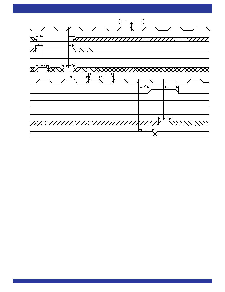
1. tSKEW1 is the minimum time between a rising CLKC edge and a rising CLKA edge for ORA to transition HIGH and to clock the next word to the FIFO2 output register in three CLKA cycles.
If the time between the CLKC edge and the rising CLKA edge is less than tSKEW1, then the transition of ORA HIGH and load of the first word to the output register may occur one CLKA
cycle later than shown.
2. If Port C size is word or byte, tSKEW1 is referenced to the rising CLKC edge that writes the last word or byte write of the long word, respectively.
Figure 18. ORA Flag Timing and First Data Word Fall through when FIFO2 is Empty (FWFT Mode)
MBC
C0-C17
CLKA
CSA
W/RA
MBA
WENC
ENA
A0-A35
CLKC
12
5611 drw19
tCLKH
tCLKL
tCLK
tENS2
tENH
tDS
tDH
tSKEW1
tCLK
tCLKL
tENS2
tENH
tA
W1
FIFO2 Empty
LOW
tCLKH
HIGH
(1)
tREF
tDH
tDS
Write 1
Write 2
ORA
IRC
3
Old Data in FIFO2 Output Register
tREF
相關PDF資料 |
PDF描述 |
|---|---|
| MS27656T15F15PB | CONN RCPT 15POS WALL MNT W/PINS |
| VE-BWN-MW-F2 | CONVERTER MOD DC/DC 18.5V 100W |
| MAX1082BEUE+T | IC ADC 10BIT 400KSPS 16-TSSOP |
| VE-BWN-MW-F1 | CONVERTER MOD DC/DC 18.5V 100W |
| ISL4485EIBZ-T | IC TXRX 1TX/1RX 5V RS-485 8-SOIC |
相關代理商/技術參數(shù) |
參數(shù)描述 |
|---|---|
| IDT72401L10DB | 制造商:Integrated Device Technology Inc 功能描述:IC FIFO ASYNC 64X4 16CDIP |
| IDT72401L10P | 功能描述:IC FIFO PAR 64X4 10NS 16-DIP RoHS:否 類別:集成電路 (IC) >> 邏輯 - FIFO 系列:7200 標準包裝:80 系列:7200 功能:同步 存儲容量:18.4K(1K x 18) 數(shù)據(jù)速率:- 訪問時間:10ns 電源電壓:4.5 V ~ 5.5 V 工作溫度:0°C ~ 70°C 安裝類型:表面貼裝 封裝/外殼:64-LQFP 供應商設備封裝:64-TQFP(10x10) 包裝:托盤 其它名稱:72225LB10TF |
| IDT72401L10SO | 功能描述:IC FIFO PAR 64X4 10NS 16-SOIC RoHS:否 類別:集成電路 (IC) >> 邏輯 - FIFO 系列:7200 標準包裝:80 系列:7200 功能:同步 存儲容量:18.4K(1K x 18) 數(shù)據(jù)速率:- 訪問時間:10ns 電源電壓:4.5 V ~ 5.5 V 工作溫度:0°C ~ 70°C 安裝類型:表面貼裝 封裝/外殼:64-LQFP 供應商設備封裝:64-TQFP(10x10) 包裝:托盤 其它名稱:72225LB10TF |
| IDT72401L10SO8 | 功能描述:IC FIFO PAR 64X4 10NS 16-SOIC RoHS:否 類別:集成電路 (IC) >> 邏輯 - FIFO 系列:7200 標準包裝:80 系列:7200 功能:同步 存儲容量:18.4K(1K x 18) 數(shù)據(jù)速率:- 訪問時間:10ns 電源電壓:4.5 V ~ 5.5 V 工作溫度:0°C ~ 70°C 安裝類型:表面貼裝 封裝/外殼:64-LQFP 供應商設備封裝:64-TQFP(10x10) 包裝:托盤 其它名稱:72225LB10TF |
| IDT72401L15DB | 制造商:Integrated Device Technology Inc 功能描述:IC FIFO ASYNC 64X4 16CDIP |
發(fā)布緊急采購,3分鐘左右您將得到回復。