- 您現(xiàn)在的位置:買賣IC網(wǎng) > PDF目錄377264 > IDT7016S15PFB (Integrated Device Technology, Inc.) HIGH-SPEED 16K x 9 DUAL-PORT STATIC RAM PDF資料下載
參數(shù)資料
| 型號(hào): | IDT7016S15PFB |
| 廠商: | Integrated Device Technology, Inc. |
| 英文描述: | HIGH-SPEED 16K x 9 DUAL-PORT STATIC RAM |
| 中文描述: | 高速16K的× 9雙端口靜態(tài)RAM |
| 文件頁(yè)數(shù): | 12/20頁(yè) |
| 文件大?。?/td> | 262K |
| 代理商: | IDT7016S15PFB |
第1頁(yè)第2頁(yè)第3頁(yè)第4頁(yè)第5頁(yè)第6頁(yè)第7頁(yè)第8頁(yè)第9頁(yè)第10頁(yè)第11頁(yè)當(dāng)前第12頁(yè)第13頁(yè)第14頁(yè)第15頁(yè)第16頁(yè)第17頁(yè)第18頁(yè)第19頁(yè)第20頁(yè)
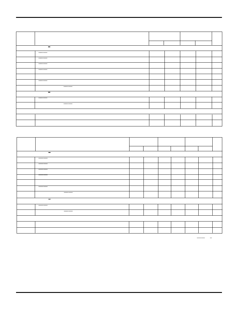
6.13
12
IDT7016S/L
HIGH-SPEED 16K x 9 DUAL-PORT STATIC RAM
MILITARY AND COMMERCIAL TEMPERATURE RANGES
BUSY TIMING (M/
S
= V
IL
)
BUSY
Input to Write
(4)
Write Hold After
BUSY
(5)
t
WB
0
—
0
—
0
—
ns
t
WH
15
—
17
—
25
—
ns
PORT-TO-PORT DELAY TIMING
Write Pulse to Data Delay
(1)
Write Data Valid to Read Data Delay
(1)
NOTES:
1. Port-to-port delay through RAM cells from writing port to reading port, refer to "Timing Waveformof Write with Port-to-Port Read and
BUSY
(M/
S
= V
IH
)".
2. To ensure that the earlier of the two ports wins.
3. t
BDD
is a calculated parameter and is the greater of 0, t
WDD
– t
WP
(actual), or t
DDD
– t
DW
(actual).
4. To ensure that the write cycle is inhibited on port "B" during contention on port "A".
5. To ensure that a write cycle is completed on port "B" after contention on port "A".
6. "X" in part numbers indicates power rating (S or L).
t
WDD
—
45
—
50
—
60
ns
t
DDD
—
30
—
30
—
35
ns
IDT7016X20
IDT7016X25
IDT7016X35
Symbol
BUSY TIMING (M/
S
= V
IH
)
t
BAA
BUSY
Access Time from Address Match
t
BDA
BUSY
Disable Time from Address Not Matched
t
BAC
BUSY
Access Time from Chip Enable Low
t
BDC
BUSY
Disable Time from Chip Enable High
Arbitration Priority Set-up Time
(2)
BUSY
Disable to Valid Data
(3)
Write Hold After
BUSY
(5)
Parameter
Min.
Max.
Min.
Max.
Min.
Max.
Unit
—
—
—
17
20
20
20
—
—
—
—
17
20
20
20
—
—
—
—
20
20
20
20
ns
ns
ns
ns
—
t
APS
5
—
5
—
5
—
ns
t
BDD
—
30
—
30
—
35
ns
t
WH
15
—
17
—
25
—
ns
AC ELECTRICAL CHARACTERISTICS OVER THE
OPERATING TEMPERATURE AND SUPPLY VOLTAGE RANGE
(6)
IDT7016X12
Com'l. Only
Min.
IDT7016X15
Com'l. Only
Min.
Symbol
BUSY TIMING (M/
S
= V
IH
)
t
BAA
BUSY
Access Time from Address Match
t
BDA
BUSY
Disable Time from Address Not Matched
t
BAC
BUSY
Access Time from Chip Enable Low
t
BDC
BUSY
Disable Time from Chip Enable High
t
APS
Arbitration Priority Set-up Time
(2)
t
BDD
BUSY
Disable to Valid Data
(3)
t
WH
Write Hold After
BUSY
(5)
Parameter
Max.
Max.
Unit
—
—
—
—
5
—
11
12
12
12
12
—
15
—
—
—
—
—
5
—
13
15
15
15
15
—
18
—
ns
ns
ns
ns
ns
ns
ns
BUSY TIMING (M/
S
= V
IL
)
t
WB
BUSY
Input to Write
(4)
Write Hold After
BUSY
(5)
PORT-TO-PORT DELAY TIMING
Write Pulse to Data Delay
(1)
Write Data Valid to Read Data Delay
(1)
0
—
0
—
ns
t
WH
11
—
13
—
ns
t
WDD
—
25
—
30
ns
t
DDD
—
20
—
25
ns
2940 tbl 13
相關(guān)PDF資料 |
PDF描述 |
|---|---|
| IDT7024 | HIGH-SPEED 4K x 16 DUAL-PORT STATIC RAM |
| IDT7024S17JB | GIGATRUE 550 CAT PATCH CBL NO BOOT 10FT YW 25 PK |
| IDT7024L17JB | GIGATRUE 550 CAT PATCH CABLE NO BOOT 15FT YELLOW |
| IDT7024L55F | HIGH-SPEED 4K x 16 DUAL-PORT STATIC RAM |
| IDT7024L55FB | HIGH-SPEED 4K x 16 DUAL-PORT STATIC RAM |
相關(guān)代理商/技術(shù)參數(shù) |
參數(shù)描述 |
|---|---|
| IDT7016S15PFG | 制造商:IDT 制造商全稱:Integrated Device Technology 功能描述:HIGH-SPEED 16K X 9 DUAL-PORT STATIC RAM |
| IDT7016S15PFGB | 制造商:IDT 制造商全稱:Integrated Device Technology 功能描述:HIGH-SPEED 16K X 9 DUAL-PORT STATIC RAM |
| IDT7016S15PFGI | 制造商:IDT 制造商全稱:Integrated Device Technology 功能描述:HIGH-SPEED 16K X 9 DUAL-PORT STATIC RAM |
| IDT7016S17J | 制造商:未知廠家 制造商全稱:未知廠家 功能描述:x9 Dual-Port SRAM |
| IDT7016S17PF | 制造商:未知廠家 制造商全稱:未知廠家 功能描述:x9 Dual-Port SRAM |
發(fā)布緊急采購(gòu),3分鐘左右您將得到回復(fù)。