- 您現(xiàn)在的位置:買賣IC網(wǎng) > PDF目錄353469 > IDT7012L55CB x9 Dual-Port SRAM PDF資料下載
參數(shù)資料
| 型號(hào): | IDT7012L55CB |
| 英文描述: | x9 Dual-Port SRAM |
| 中文描述: | X9熱賣雙端口SRAM |
| 文件頁(yè)數(shù): | 14/15頁(yè) |
| 文件大小: | 190K |
| 代理商: | IDT7012L55CB |
第1頁(yè)第2頁(yè)第3頁(yè)第4頁(yè)第5頁(yè)第6頁(yè)第7頁(yè)第8頁(yè)第9頁(yè)第10頁(yè)第11頁(yè)第12頁(yè)第13頁(yè)當(dāng)前第14頁(yè)第15頁(yè)
6.42
IDT70V9379L
High-Speed 32K x 18 Dual-Port Synchronous Pipelined Static RAM
Industrial and Commercial Temperature Ranges
8
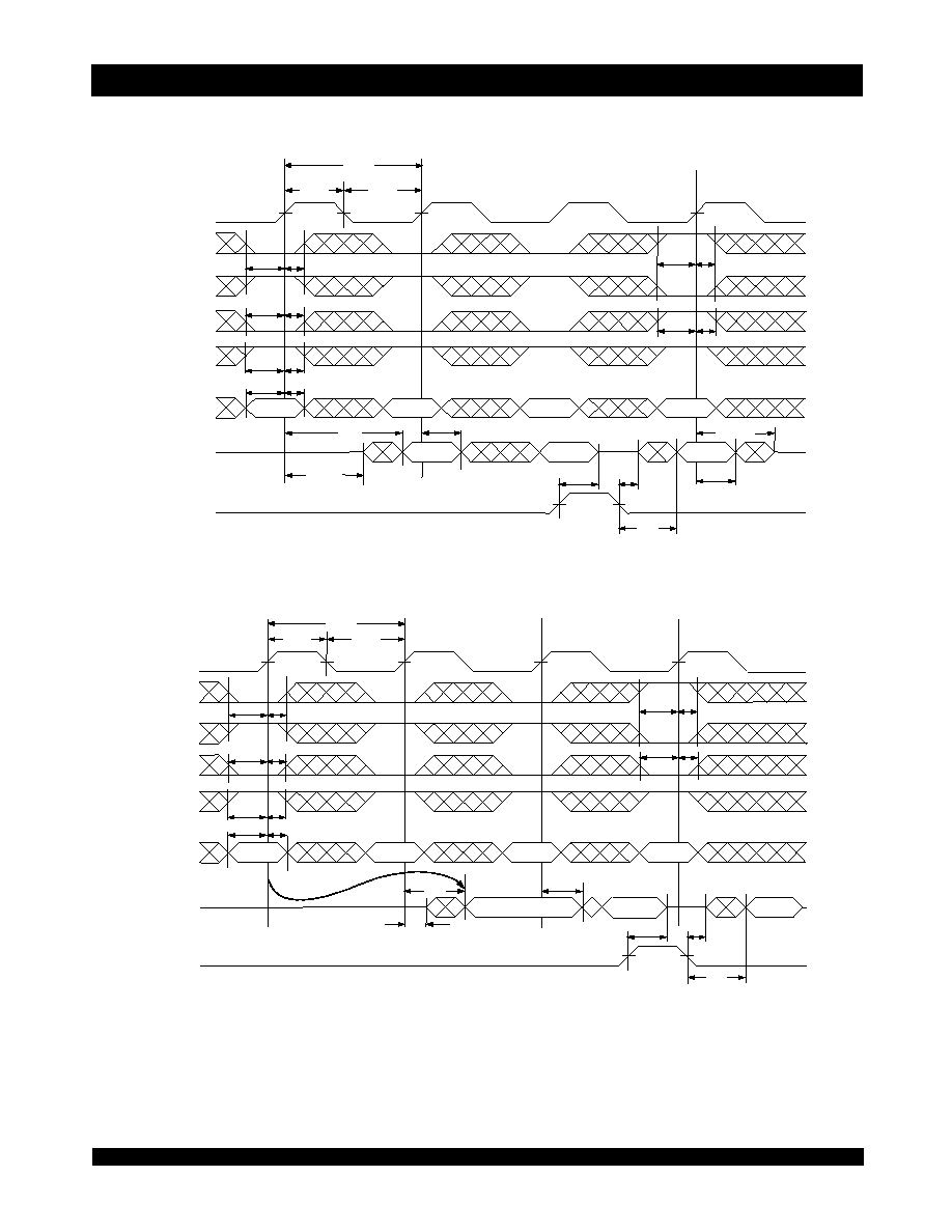
Timing Waveform of Read Cycle for Flow-Through Output
(FT/PIPE"X" = VIL)(3,7)
Timing Waveform of Read Cycle for Pipelined Operation
(FT/PIPE"X" = VIH)(3,7)
An
An + 1
An + 2
An + 3
tCYC1
tCH1
tCL1
R/W
ADDRESS
DATAOUT
CE0
CLK
OE
tSC
tHC
tCD1
tCKLZ
Qn
Qn + 1
Qn + 2
tOHZ
tOLZ
tOE
tCKHZ
4857 drw 06
(1)
(2)
CE1
UB, LB
(4)
tSB
tHB
tSW
tHW
tSA
tHA
tDC
(5)
tSC
tHC
tSB
tHB
An
An + 1
An + 2
An + 3
tCYC2
tCH2
tCL2
R/W
ADDRESS
CE0
CLK
CE1
UB, LB
(4)
DATAOUT
OE
tCD2
tCKLZ
Qn
Qn + 1
Qn + 2
tOHZ
tOLZ
tOE
4857 drw 07
(1)
(2)
tSC
tHC
tSB
tHB
tSW
tHW
tSA
tHA
tDC
tSC
tHC
tSB
tHB
(5)
(1 Latency)
(6)
NOTES:
1. Transition is measured 0mV from Low or High-impedance voltage with the Output Test Load (Figure 2).
2.
OE is asynchronously controlled; all other inputs are synchronous to the rising clock edge.
3.
ADS = VIL, CNTEN and CNTRST = VIH.
4. The output is disabled (High-Impedance state) by
CE0 = VIH, CE1 = VIL, UB = VIH, or LB = VIH following the next rising edge of the clock. Refer to Truth Table 1.
5. Addresses do not have to be accessed sequentially since ADS = VIL constantly loads the address on the rising edge of the CLK; numbers
are for reference use only.
6. If
UB or LB was HIGH, then the Upper Byte and/or Lower Byte of DATAOUT for Qn + 2 would be disabled (High-Impedance state).
7. "X' here denotes Left or Right port. The diagram is with respect to that port.
相關(guān)PDF資料 |
PDF描述 |
|---|---|
| IDT7012L55F | x9 Dual-Port SRAM |
| IDT7012L55FB | x9 Dual-Port SRAM |
| IDT7012L55L48 | x9 Dual-Port SRAM |
| IDT7012L55L48B | x9 Dual-Port SRAM |
| IDT7012L55P | x9 Dual-Port SRAM |
相關(guān)代理商/技術(shù)參數(shù) |
參數(shù)描述 |
|---|---|
| IDT7012L55F | 制造商:未知廠家 制造商全稱:未知廠家 功能描述:x9 Dual-Port SRAM |
| IDT7012L55FB | 制造商:未知廠家 制造商全稱:未知廠家 功能描述:x9 Dual-Port SRAM |
| IDT7012L55L48 | 制造商:未知廠家 制造商全稱:未知廠家 功能描述:x9 Dual-Port SRAM |
| IDT7012L55L48B | 制造商:未知廠家 制造商全稱:未知廠家 功能描述:x9 Dual-Port SRAM |
| IDT7012L55P | 制造商:未知廠家 制造商全稱:未知廠家 功能描述:x9 Dual-Port SRAM |
發(fā)布緊急采購(gòu),3分鐘左右您將得到回復(fù)。