- 您現(xiàn)在的位置:買賣IC網(wǎng) > PDF目錄360752 > ICS650-07B Broadcom Clock Source PDF資料下載
參數(shù)資料
| 型號: | ICS650-07B |
| 英文描述: | Broadcom Clock Source |
| 中文描述: | Broadcom的時鐘源 |
| 文件頁數(shù): | 1/4頁 |
| 文件大?。?/td> | 46K |
| 代理商: | ICS650-07B |
ICS650-07B
Broadcom Clock Source
MD S 650-07B A
Integrated Circuit Systems, Inc. 525 Race Street San Jose CA 95126(408)295-9800tel www.icst.com
1
Revision 042600
Printed 11/15/00
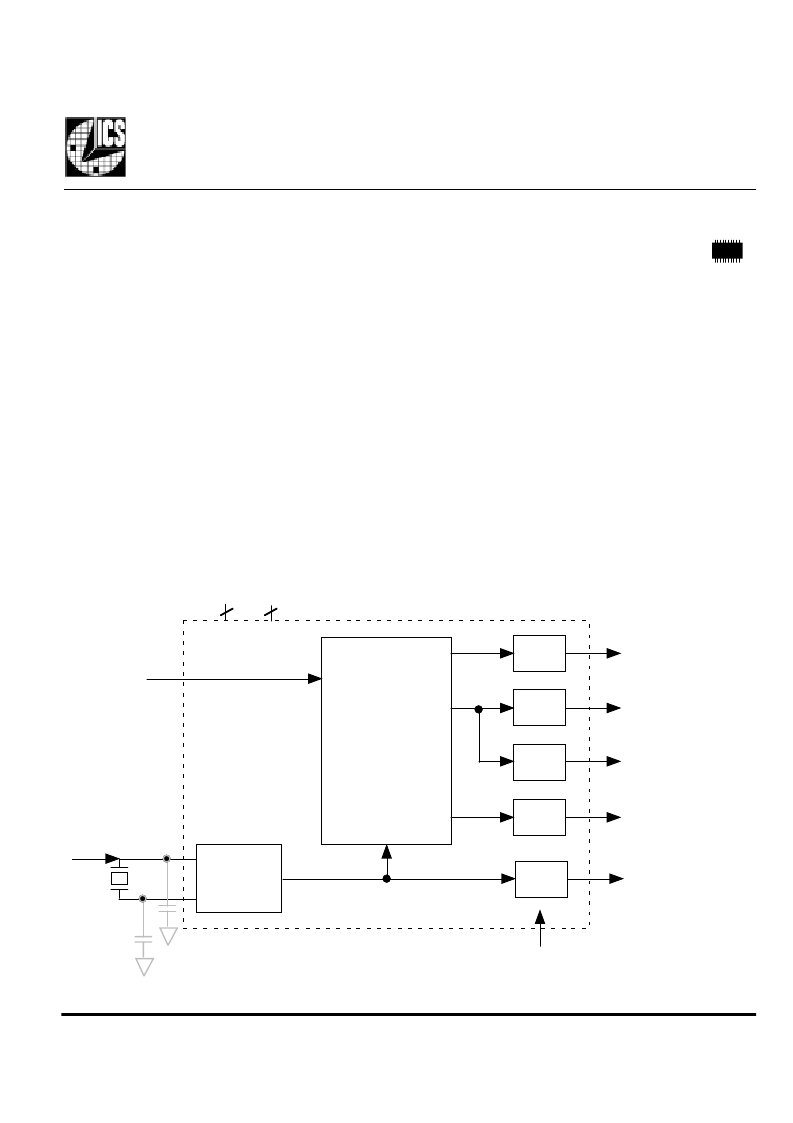
The ICS650-07B is a low cost, low jitter, high
performance clock synthesizer customized for
Broadcom. Using analog Phase-Locked Loop
(PLL) techniques, the device accepts a 25.00 MHz
clock or fundamental mode crystal input to
produce multiple output clocks of 25.0 MHz, two
125.0 MHz, 133.33 MHz, and a selectable
33.3/66.6 MHz clock. All output clocks are
frequency locked together. The ICS650-07B
outputs all have 0 ppm synthesis error.
Do not use the 125 MHz outputs to drive Gigabit
Ethernet SERDES. Instead, the 25 MHz clock
can be driven into our ICS601 in the X5 mode.
The ICS601 has low enough jitter and phase noise
for all popular SERDES.
Block Diagram
VDD
Description
Features
Packaged in 20 pin narrow (150 mil) SSOP (QSOP)
25.00 MHz fundamental crystal or clock input
Four fixed output clocks of 25 MHz, 133.33 MHz,
and two copies of 125 MHz
One selectable output clock of 33.3 or 66.6 MHz
Zero ppm synthesis error in all clocks
PCI clock switching occurs within 1
μ
s
Ideal for Broadcom’s BCM5600 chipset
Full CMOS output swing
Advanced, low power, sub-micron CMOS process
3.0 V to 5.5 V operating voltage
Clock
Buffer/
Crystal
Oscillator
GND
Clock Synthesis
and Control
Circuitry
133.33 MHz
25.00 MHz
crystal or clock
X1
Output
Buffer
Output
Buffer
125.00 MHz
25.00 MHz
4
3
Output
Buffer
125.00 MHz
Output
Buffer
X2
Output
Buffer
PCI CLK
Optional crystal capacitors are shown and may be required for tuning of initial accuracy (determined once per board).
PS
OE (all outputs)
相關(guān)PDF資料 |
PDF描述 |
|---|---|
| ICS650-07C | Networking Clock Source |
| ICS650-11B | BroadCom Networking Clock Synthesizer |
| ICS650R-11I | BroadCom Networking Clock Synthesizer |
| ICS650R-11IT | BroadCom Networking Clock Synthesizer |
| ICS650-14B | Networking System Clock |
相關(guān)代理商/技術(shù)參數(shù) |
參數(shù)描述 |
|---|---|
| ICS650-07C | 制造商:ICS 制造商全稱:ICS 功能描述:Networking Clock Source |
| ICS650-11B | 制造商:ICS 制造商全稱:ICS 功能描述:BroadCom Networking Clock Synthesizer |
| ICS650-12 | 制造商:ICS 制造商全稱:ICS 功能描述:MPEG Clock Synthesizer |
| ICS650-14B | 制造商:ICS 制造商全稱:ICS 功能描述:Networking System Clock |
| ICS650-21 | 制造商:ICS 制造商全稱:ICS 功能描述:System Peripheral Clock Source |
發(fā)布緊急采購,3分鐘左右您將得到回復(fù)。