- 您現(xiàn)在的位置:買(mǎi)賣(mài)IC網(wǎng) > PDF目錄385435 > HYS72T128020HU-3S-B (QIMONDA AG) 240-Pin unbuffered DDR2 SDRAM Modules PDF資料下載
參數(shù)資料
| 型號(hào): | HYS72T128020HU-3S-B |
| 廠商: | QIMONDA AG |
| 元件分類(lèi): | DRAM |
| 英文描述: | 240-Pin unbuffered DDR2 SDRAM Modules |
| 中文描述: | 128M X 72 DDR DRAM MODULE, 0.45 ns, DMA240 |
| 封裝: | GREEN, UDIMM-240 |
| 文件頁(yè)數(shù): | 24/87頁(yè) |
| 文件大小: | 1723K |
| 代理商: | HYS72T128020HU-3S-B |
第1頁(yè)第2頁(yè)第3頁(yè)第4頁(yè)第5頁(yè)第6頁(yè)第7頁(yè)第8頁(yè)第9頁(yè)第10頁(yè)第11頁(yè)第12頁(yè)第13頁(yè)第14頁(yè)第15頁(yè)第16頁(yè)第17頁(yè)第18頁(yè)第19頁(yè)第20頁(yè)第21頁(yè)第22頁(yè)第23頁(yè)當(dāng)前第24頁(yè)第25頁(yè)第26頁(yè)第27頁(yè)第28頁(yè)第29頁(yè)第30頁(yè)第31頁(yè)第32頁(yè)第33頁(yè)第34頁(yè)第35頁(yè)第36頁(yè)第37頁(yè)第38頁(yè)第39頁(yè)第40頁(yè)第41頁(yè)第42頁(yè)第43頁(yè)第44頁(yè)第45頁(yè)第46頁(yè)第47頁(yè)第48頁(yè)第49頁(yè)第50頁(yè)第51頁(yè)第52頁(yè)第53頁(yè)第54頁(yè)第55頁(yè)第56頁(yè)第57頁(yè)第58頁(yè)第59頁(yè)第60頁(yè)第61頁(yè)第62頁(yè)第63頁(yè)第64頁(yè)第65頁(yè)第66頁(yè)第67頁(yè)第68頁(yè)第69頁(yè)第70頁(yè)第71頁(yè)第72頁(yè)第73頁(yè)第74頁(yè)第75頁(yè)第76頁(yè)第77頁(yè)第78頁(yè)第79頁(yè)第80頁(yè)第81頁(yè)第82頁(yè)第83頁(yè)第84頁(yè)第85頁(yè)第86頁(yè)第87頁(yè)
Internet Data Sheet
Rev. 1.3, 2006-12
03292006-6GMD-RSFT
24
HYS[64/72]T[32/64/128]xx0HU-[25F/2.5/3/3S/3.7/5]-B
Unbuffered DDR2 SDRAM Module
DQ and DM input setup time
DQS falling edge hold time from CK
DQS falling edge to CK setup time
CK half pulse width
t
DS.BASE
t
DSH
t
DSS
t
HP
100
0.2
0.2
Min(
t
CH.ABS
,
t
CL.ABS
)
—
275
0.6
200
2 x
t
AC.MIN
t
AC.MIN
0
2
0
t
HP
–
t
QHS
—
0.9
0.4
7.5
0.35
0.4
15
7.5
2
7 – AL
—
—
—
—
ps
t
CK.AVG
t
CK.AVG
ps
18)19)20)
17)
17)
21)
Data-out high-impedance time from CK / CK
Address and control input hold time
Control & address input pulse width for each input
t
IPW
Address and control input setup time
DQ low impedance time from CK/CK
DQS/DQS low-impedance time from CK / CK
MRS command to ODT update delay
Mode register set command cycle time
OCD drive mode output delay
DQ/DQS output hold time from DQS
DQ hold skew factor
Read preamble
Read postamble
Internal Read to Precharge command delay
Write preamble
Write postamble
Write recovery time
Internal write to read command delay
Exit power down to read command
Exit active power-down mode to read command
(slow exit, lower power)
Exit precharge power-down to any valid
command (other than NOP or Deselect)
Exit self-refresh to a non-read command
Exit self-refresh to read command
Write command to DQS associated clock edges
1) For details and notes see the relevant Qimonda component data sheet
2)
V
DDQ
= 1.8 V ± 0.1V;
V
DD
= 1.8 V ± 0.1 V. See notes
5)6)7)8)
3) Timing that is not specified is illegal and after such an event, in order to guarantee proper operation, the DRAM must be powered down
and then restarted through the specified initialization sequence before normal operation can continue.
4) Timings are guaranteed with CK/CK differential Slew Rate of 2.0 V/ns. For DQS signals timings are guaranteed with a differential Slew
Rate of 2.0 V/ns in differential strobe mode and a Slew Rate of 1 V/ns in single ended mode.
5) The CK / CK input reference level (for timing reference to CK / CK) is the point at which CK and CK cross. The DQS / DQS, RDQS / RDQS,
input reference level is the crosspoint when in differential strobe mode.
6) Inputs are not recognized as valid until
V
REF
stabilizes. During the period before
V
REF
stabilizes, CKE = 0.2 x
V
DDQ
is recognized as low.
7) The output timing reference voltage level is
V
TT
.
t
HZ
t
IH.BASE
t
AC.MAX
—
—
—
t
AC.MAX
t
AC.MAX
12
—
12
—
340
1.1
0.6
—
—
0.6
—
—
—
—
ps
ps
t
CK.AVG
ps
ps
ps
ns
nCK
ns
ps
ps
t
CK.AVG
t
CK.AVG
ns
t
CK.AVG
t
CK.AVG
ns
ns
nCK
nCK
9)22)
25)23)
t
IS.BASE
t
LZ.DQ
t
LZ.DQS
t
MOD
t
MRD
t
OIT
t
QH
t
QHS
t
RPRE
t
RPST
t
RTP
t
WPRE
t
WPST
t
WR
t
WTR
t
XARD
t
XARDS
24)25)
9)22)
9)22)
31)
31)
26)
27)
28)29)
28)30)
31)
31)
31)32)
t
XP
2
—
nCK
t
XSNR
t
XSRD
WL
t
RFC
+10
200
RL–1
—
—
ns
nCK
nCK
31)
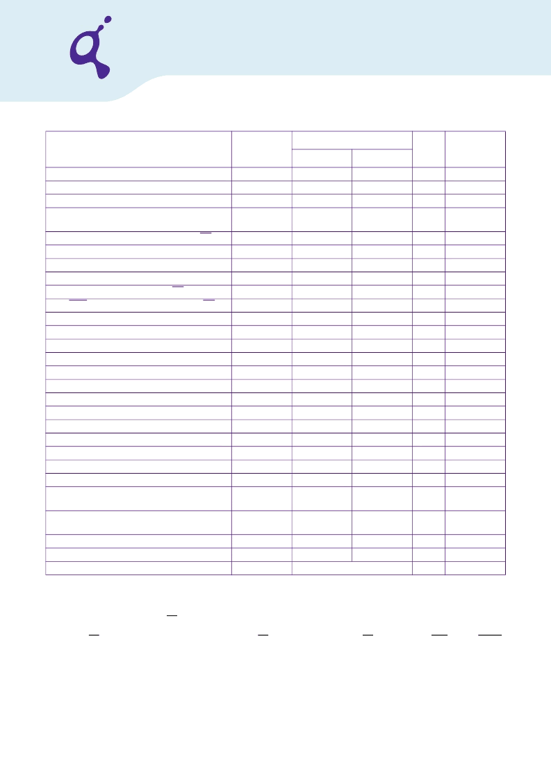
Parameter
Symbol
DDR2–667
Unit
Note
1)2)3)4)5)6)7)8)
Min.
Max.
相關(guān)PDF資料 |
PDF描述 |
|---|---|
| HYS72T128020HU-5-B | 240-Pin unbuffered DDR2 SDRAM Modules |
| HYS72T64000HU-2.5-B | 240-Pin unbuffered DDR2 SDRAM Modules |
| HYS72T64000HU-25F-B | 240-Pin unbuffered DDR2 SDRAM Modules |
| HYS72T64000HU-3.7-B | 240-Pin unbuffered DDR2 SDRAM Modules |
| HYS72T64000HU-3-B | 240-Pin unbuffered DDR2 SDRAM Modules |
相關(guān)代理商/技術(shù)參數(shù) |
參數(shù)描述 |
|---|---|
| HYS72T128020HU-5-A | 制造商:QIMONDA 制造商全稱:QIMONDA 功能描述:240-Pin Unbuffered DDR2 SDRAM Modules |
| HYS72T128020HU-5-B | 制造商:QIMONDA 制造商全稱:QIMONDA 功能描述:240-Pin unbuffered DDR2 SDRAM Modules |
| HYS72T128300HP-3.7-A | 制造商:QIMONDA 制造商全稱:QIMONDA 功能描述:240-Pin Registered DDR2 SDRAM Modules |
| HYS72T128300HP-3S-A | 制造商:QIMONDA 制造商全稱:QIMONDA 功能描述:240-Pin Registered DDR2 SDRAM Modules |
| HYS72T128320HP-3.7-A | 制造商:QIMONDA 制造商全稱:QIMONDA 功能描述:240-Pin Registered DDR2 SDRAM Modules |
發(fā)布緊急采購(gòu),3分鐘左右您將得到回復(fù)。