- 您現(xiàn)在的位置:買賣IC網(wǎng) > PDF目錄370732 > HWD2119 (Electronic Theatre Controls, Inc.) 350mWAudio Power Amplifier with Shutdown Mode PDF資料下載
參數(shù)資料
| 型號: | HWD2119 |
| 廠商: | Electronic Theatre Controls, Inc. |
| 英文描述: | 350mWAudio Power Amplifier with Shutdown Mode |
| 中文描述: | 350mWAudio功率放大器關(guān)斷模式 |
| 文件頁數(shù): | 11/21頁 |
| 文件大小: | 877K |
| 代理商: | HWD2119 |

Application Information
(Continued)
In order to eliminate ’clicks and pops’, all capacitors must be
discharged before turn-on. Rapidly switching V
may not
allow the capacitors to fully discharge, which may cause
’clicks and pops’.
AUDIO POWER AMPLIFIER DESIGN EXAMPLE
The following are the desired operational
parameters:
Given:
Power Output
Load Impedance
Input Level
Input Impedance
Bandwidth
The design begins by specifying the minimum supply voltage
necessary to obtain the specified output power. To find this
minimum supply voltage, use the
Output Power vs. Supply
Voltage
graph in the
Typical Performance Characteristics
section. From the graph for a 16
load, (graphs are for 8
,
16
, and 32
loads) the supply voltage for 100mW of output
power with 1% THD+N is approximately 3.15 volts.
Additional supply voltage creates the benefit of increased
headroom that allows the
HWD
21
19 to reproduce peaks in
excess of 100mW without output signal clipping or audible
distortion. The choice of supply voltage must also not create
a situation that violates maximum dissipation as explained
above in the
Power Dissipation
section. For example, if a
3.3V supply is chosen for extra headroom then according to
Equation (3) the maximum power dissipation point with a
16
load is 138mW. Using Equation (4) the maximum am-
bient temperature is 121C for the MUA08A package and
126C for the M08A package.
After satisfying the
HWD
21
19’s power dissipation require-
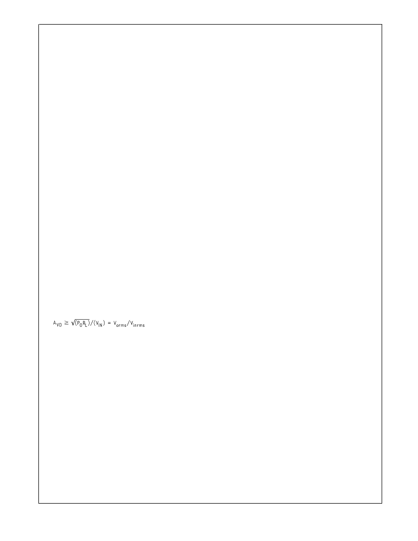
ments, the minimum differential gain is found using Equation
(6).
100mW
16
1Vrms (max)
20k
100Hz–20kHz
±
0.25dB
(6)
Thus a minimum gain of 1.27 V/V allows the
HWD
21
19 to
reach full output swing and maintain low noise and THD+N
performance. For this example, let A
= 1.27. The amplifi-
er’s overall gain is set using the input (R
) and feedback (R
)
resistors. With the desired input impedance set to 20k
, the
feedback resistor is found using Equation (7).
R
F
/R
i
= A
VD
/2 (V/V)
The value of R
F
is 13k
.
(7)
The last step in this design example is setting the amplifier’s
-3dB frequency bandwidth. To achieve the desired
±
0.25dB
pass band magnitude variation limit, the low frequency re-
sponse must extend to at least one-fifth the lower bandwidth
limit and the high frequency response must extend to at least
five times the upper bandwidth limit. The gain variation for
both response limits is 0.17dB, well with in the
±
0.25dB
desired limit.
The results are:
f
L
= 100Hz/5 = 20Hz
f
H
= 20 kHz*5 = 100kHz
As mentioned in the
External Components
section, R
and
C
create a high pass filter that sets the amplifier’s lower
band pass frequency limit. Find the coupling capacitor’s
value using Equation (8).
C
i
≥
1/(2
π
R
i
f
c
) (F)
(8)
C
≥
0.398μF, a standard value of 0.39μF will be used. The
product of the desired high frequency cutoff (100kHz in this
example) and the differential gain, A
, determines the up-
per pass band response limit. With A
= 1.27 and f
=
100kHz, the closed-loop gain bandwidth product (GBWP) is
127kHz. This is less than the
HWD
21
19’s 900kHz GBWP. With
this margin the amplifier can be used in designs that require
more differential gain while avoiding performance restricting
bandwidth limitations.
11
相關(guān)PDF資料 |
PDF描述 |
|---|---|
| HWD4558 | DUAL OPERATIONAL AMPLIFIERS |
| HWD4558M | DUAL OPERATIONAL AMPLIFIERS |
| HWD4558P | DUAL OPERATIONAL AMPLIFIERS |
| HWD490 | Low-Power, Slew-Rate-Limited RS-485/RS-422 Transceivers |
| HWD490CPA | Low-Power, Slew-Rate-Limited RS-485/RS-422 Transceivers |
相關(guān)代理商/技術(shù)參數(shù) |
參數(shù)描述 |
|---|---|
| HWD2171 | 制造商:未知廠家 制造商全稱:未知廠家 功能描述:低電壓放大器 |
| HWD2182 | 制造商:未知廠家 制造商全稱:未知廠家 功能描述:250mW Audio Power Amplifier with Shutdown Mode |
| HWD2190 | 制造商:未知廠家 制造商全稱:未知廠家 功能描述:1 Watt Audio Power Amplifier |
| HWD22 | 制造商:NTE Electronics 功能描述: |
| HWD232 | 制造商:未知廠家 制造商全稱:未知廠家 功能描述:+5V RS-232 |
發(fā)布緊急采購,3分鐘左右您將得到回復(fù)。