- 您現在的位置:買賣IC網 > PDF目錄370725 > HV3-2405E-5 (Harris Corporation) World-Wide Single Chip Power Supply PDF資料下載
參數資料
| 型號: | HV3-2405E-5 |
| 廠商: | Harris Corporation |
| 英文描述: | World-Wide Single Chip Power Supply |
| 中文描述: | 環(huán)球單片電源 |
| 文件頁數: | 11/14頁 |
| 文件大小: | 573K |
| 代理商: | HV3-2405E-5 |

5-25
HV-2405E
Safe Operating Area
Ensure operation is within the SOA of the HV-2405E. Refer-
ence “Start-Up” in section titled “How the HV-2405E Works”.
How The HV-2405E Works
Steady State Operation
The HV-2405E converts an AC voltage into a regulated DC
voltage. This is accomplished in two functional sections (1)
Switching Pre-Regulator and (2) Linear Voltage Regulator.
Refer to HV-2405E schematic Figure 16.
The purpose of the Switching Pre-Regulator circuit is to cap-
ture energy from an incoming AC power line, 1/6 of every
positive half cycle and store this energy in an electrolytic
capacitor (C2). This energy is then transferred to the Linear
Voltage Regulator.The current path for charging C2 is
through DA1, SA1 and DA2. When the voltage level on C2
reaches approximately 6.8V above the output voltage, SA2
turns on turning off SA1 and the charging of C2 stops until
the next positive half cycle on AC high. SA2 is triggered on
when current flows out of SA2s anode gate and through the
Zener diode stack (ZA1, DA3, DA4, DA5). This results in a
feedback circuit that limits the peak voltage on pin 2.
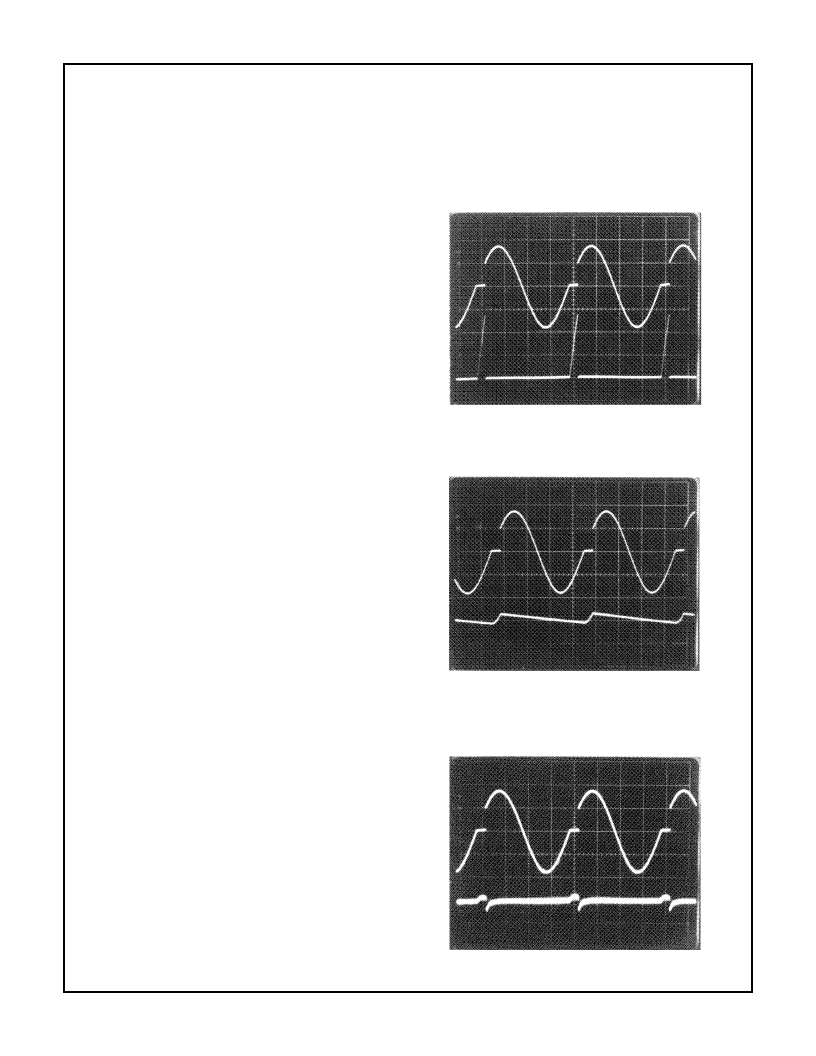
The input voltage and current wave forms at pin 8 are illus-
trated in Photo 1. The operation of the HV-2405E is easily
confirmed by noticing the clamping of the input voltage dur-
ing the charging of C2. Photo 2 shows the voltage on C2
(bottom trace), along with the voltage on pin 8 as a refer-
ence. The test conditions for the wave forms are listed at the
end of this section.
The Linear Voltage Regulator performs two functions. The
first is to provide a reference voltage at pin 5 that is tempera-
ture independent and the second is to provide an output volt-
age on pin 6 that is adjustable from 5V to 24V. The band-gap
(NB1, NB2, RB3 and RB4) provides a temperature indepen-
dent reference voltage on the base of NB5. This reference
voltage (1.21V) results in approximately 1mA through RB10
when the feedback loop from pin 6 is closed. The output volt-
age is adjusted by placing a Zener diode between pin 5 and
pin 6. The output voltage on pin 6 is adjusted above the 5V
reference on pin 5 by a value equal to the Zener voltage. The
maximum output voltage is limited to
≈
34V
DC
by the internal
Zener diode Z
B2
. Z
B2
protects the output by ensuring that an
overvoltage condition does not exist. The bottom trace of
Photo 3 shows the output voltage ripple (worst case condi-
tions), along with the voltage on pin 8 as a reference.
Test conditions for waveforms: T
A
= +25
o
C, V
AC
= 240Vrms,
f = 50Hz, R1 = 150
, C1= 0.1
μ
F, C2 = 470
μ
F, C3 = 150pF,
C4 = 1
μ
F, V
OUT
= 5V at 50mA.
Start-up
Start up operation is similar to that described above. Since
the storage capacitor connected to pin 2 is discharged, the
main SCR, SA1, has to pass more current than for steady
state.
The ability of the second SCR, SA2, to turn off SA1 is a function
of the voltage on C2. Due to the impedances of SA1 and SA2,
the maximum input current that can be safely turned off
decreases for C2 voltages below 5V. To understand why the
voltage on C2 determines the maximum input current that the
HV-2405E can safely turn off, its important to understand the
electrical connection between SA1, SA2 and the storage
capacitor C2. Figure 17(A) is a schematic representation of
both SCRs and is presented to explain how SA2 turns off SA1.
Top Trace: Input Voltage at Pin 8, AC High (200V/Div)
Bottom Trace: Current into Pin 8, (0.5A/Div)
PHOTO 1
Top Trace: Input Voltage at Pin 8, AC High (200V/Div)
Bottom Trace: Pre-Regulator Capacitor Voltage, C2
(5V/Div) at Approximately 10V
DC
PHOTO 2
Top Trace: Input Voltage at Pin 8, AC High (200V/Div)
Bottom Trace: Ripple or Switch Spike on Regulator 5V
DC
Output (50mV/Div) This is Worst Case
Ripple (High Line Voltage, Maximum I
OUT
)
PHOTO 3
相關PDF資料 |
PDF描述 |
|---|---|
| HV3-2405E-9 | World-Wide Single Chip Power Supply |
| HV3-2405E-5 | PT 21C 21#16 SKT PLUG |
| HV3-2405E-9 | World-WideSingle Chip Power Supply |
| HV341C | Interface IC |
| HV341MC | Interface IC |
相關代理商/技術參數 |
參數描述 |
|---|---|
| HV3-2405E-9 | 制造商:INTERSIL 制造商全稱:Intersil Corporation 功能描述:World-WideSingle Chip Power Supply |
| HV3-2405E-9 DIE | 制造商:Harris Corporation 功能描述: |
| HV33 | 制造商:WELWYN 制造商全稱:Welwyn Components Limited 功能描述:High Voltage Thick film Resistors |
| HV3304DJ | 制造商:未知廠家 制造商全稱:未知廠家 功能描述:Interface IC |
| HV3304PJ | 制造商:未知廠家 制造商全稱:未知廠家 功能描述:Interface IC |
發(fā)布緊急采購,3分鐘左右您將得到回復。