- 您現(xiàn)在的位置:買賣IC網(wǎng) > PDF目錄370725 > HV2405E (Harris Corporation) World-Wide Single Chip Power Supply PDF資料下載
參數(shù)資料
| 型號(hào): | HV2405E |
| 廠商: | Harris Corporation |
| 英文描述: | World-Wide Single Chip Power Supply |
| 中文描述: | 環(huán)球單片電源 |
| 文件頁數(shù): | 6/14頁 |
| 文件大?。?/td> | 573K |
| 代理商: | HV2405E |

5-20
HV-2405E
Minimum Input Voltage vs I
OUT
Table 1 shows the minimum input voltage range as a
function of output current. Notice that the HV-2405E can
deliver 5V at 10mA from a source voltage as little as 15Vrms
and requires a minimum of 50Vrms to deliver 24V at 50mA.
Component List
(World Wide Supply <50mA)
Fuse
Opens the connection to the power line.
Recommended value: 1/4AG
R1 Source Resistor
R1 limits the input current into the HV-2405E. Needs to be
large enough to limit inrush current when C2 is discharged
fully. The maximum inrush current needs to be limited to less
than 2A (V peak / R1 <2A). The equation for power dissipa-
tion in R1 is:
Wirewound resistors are recommended due to their superior
temperature characteristics.
R1 = 100
(
±
10%)
R2, R3, R4, R5 and R6 Resistors
R2, R3, R4, R5 and R6 set the bias level for Q1 that
establishes the minimum and maximum input current limit
during start-up.
Resistor values (
±
5%):
C1 Snubber Capacitor
C1 and R1 form a low pass filter that limits the voltage rate
of rise across SA1 (the main current carrying SCR of the
HV-2405E) and therefore its power dissipation.
C1 = 0.1
μ
F (
±
10%) AC rated, metallized polyester.
C2 Pre-Regulator Capacitor
C2 is charged once each line cycle. The post regulator
section of the HV-2405E is powered by C2 for most of the
line cycle. If the application requires a smaller input voltage,
the value of C2 can be reduced from that shown in Figure 1
(see section on “Optimizing Design” for details). Note:
capacitors with high ESR may not store enough charge to
maintain full load current. The voltage rating of C2 should be
about 10V greater than the selected V
OUT
.
TABLE 1. MINIMUM INPUT VOLTAGE vs OUTPUT CURRENT
I
OUT
25mA
V
OUT
5V
10mA
35mA
50mA
15Vrms
21Vrms
25Vrms
30Vrms
24V
31Vrms
38Vrms
41Vrms
50Vrms
Pd = 2.8
(EQ. 10)
R2 = 220k
, 1W
R3 = 3.9k
, 1/4W
R4 = 5.6k
, 1/4W
R5 = 3.3k
, 1/4W
R6 = 5.6k
, 1/4W
√
R1 Vrms (I
OUT
)
3
Recommended value = 470
μ
F electrolytic (
±
20%), unless
otherwise specified.
C3 Feed Forward Capacitor
C3 is part of the input Current limiting circuitry shown in
Figure 1. C3 detects large voltage transients on the AC line
and turns off the HV-2405E by turning Q1 on.
C3 = 20pF (20%), breakdown voltage >500V.
C4 Output Filter Capacitor
C4 is required to maintain the stability of the output stage.
Larger values may help in supplying short momentary
current peaks to the load and improve output ripple during
start-up.
C4 = 10
μ
F (
±
20%)
Z1 Output Voltage Adjust
Z1 is used to set the output voltage above the 5V reference
on pin 5 (see section titled “Setting The Output Voltage” for
more details).
Z1= V
OUT
- 5V,1/4W. V2 valve at 1mA.
Note, the wattage rating is different when configured as a
dual supply (see dual supply section for on how to determine
wattage).
Z2 Clamp Diode
Z2 clamps the voltage on Q1s emitter when the voltage on
C2 >10V. This results in limiting the maximum input current
to less than 2A.
Z2 = 5.1V, 1N5231A or equivalent
Q1 Input Current Limiting Transistor
Q1 shuts down the HV-2405E when the input voltage or dv/dt
is too large.
V
CEO
= 40V min.
Q1 = 2N2222 or equivalent
Imbedded Supply
(I
OUT
≤
30mA)
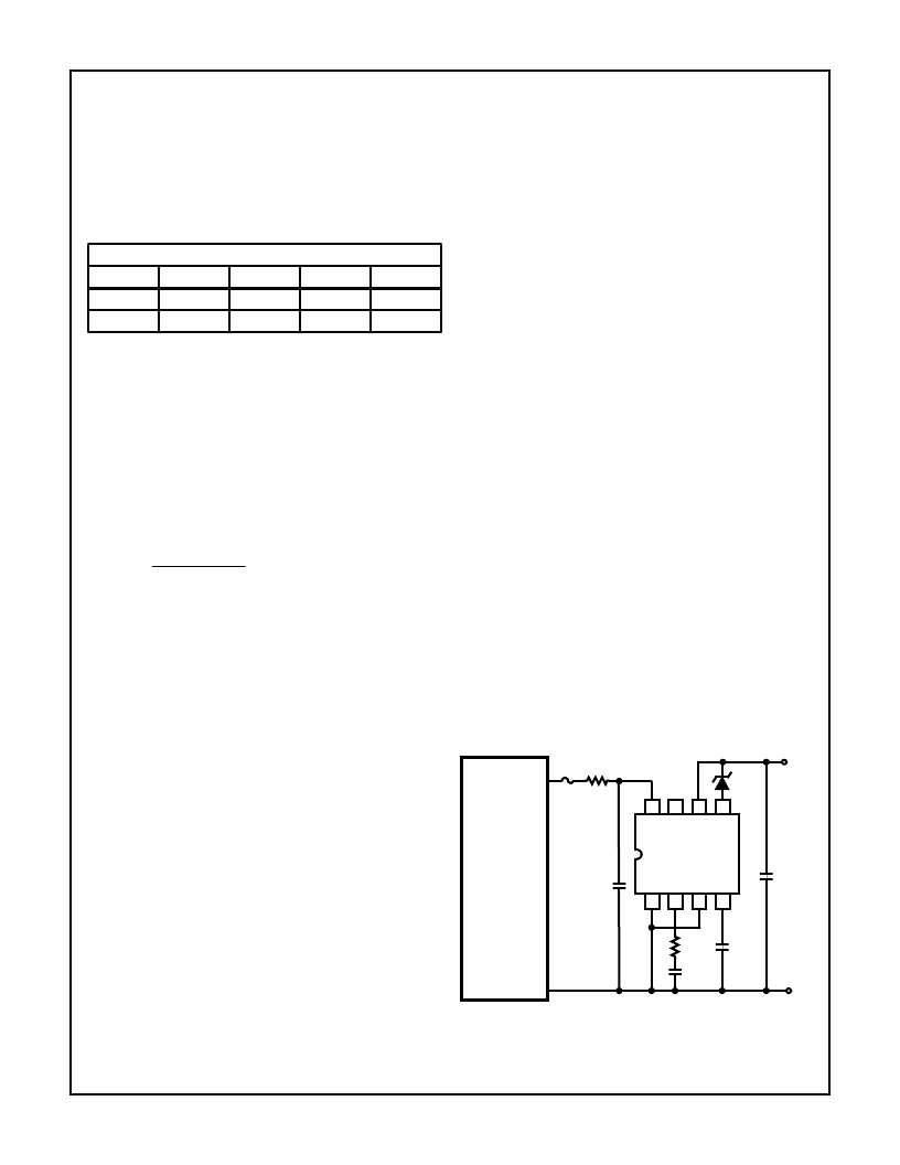
FIGURE 7. IMBEDDED SUPPLY I
OUT
≤
30mA
1
2
3
4
8
7
6
5
HV-2405E
N
C2
330
μ
F
C3
150pF
C4
10
μ
F
C1
0.1
μ
F
V
OUT
+
-
R1
150
R2
2.7
dv/dt < 10V/
μ
s
FILTER
NETWORK
COMPONENT LIST
C2 = 330
μ
F, 15V + V
OUT
, ELECTROLYTIC
C3 = 150pF, CERAMIC
C4 = 10
μ
F, V
OUT
+ 10V, ELECTROLYTIC
Z1 = V
OUT
-5V, 1/4W
FUSE = 1/4A
R1 = 150
, 3W
R2 = 2.7
, 1/4W
C1 = 0.1
μ
F, AC RATED
FUSE
Application Information
(Continued)
相關(guān)PDF資料 |
PDF描述 |
|---|---|
| HV3-2405E-5 | World-Wide Single Chip Power Supply |
| HV3-2405E-9 | World-Wide Single Chip Power Supply |
| HV3-2405E-5 | PT 21C 21#16 SKT PLUG |
| HV3-2405E-9 | World-WideSingle Chip Power Supply |
| HV341C | Interface IC |
相關(guān)代理商/技術(shù)參數(shù) |
參數(shù)描述 |
|---|---|
| HV-2405E | 制造商:HARRIS 制造商全稱:HARRIS 功能描述:World-Wide Single Chip Power Supply |
| HV250 | 制造商:TESTEC 功能描述:PROBE HIGH VOLTAGE 2.5KV 制造商:TESTEC 功能描述:PROBE, HIGH VOLTAGE, 2.5KV 制造商:TESTEC 功能描述:PROBE, HIGH VOLTAGE, 2.5KV; Test Probe Type:Various; Test Probe Functions:Voltage; For Use With:Oscilloscopes; SVHC:No SVHC (19-Dec-2012); Attenuation:x100; Bandwidth:300MHz; External Length / Height:1.2m; Input Impedance:100Mohm; |
| HV250A | 功能描述:氣體放電管 - GDT /氣體等離子體避雷器 2500V RoHS:否 制造商:Bourns 峰值脈沖電流: 直流擊穿電壓(標(biāo)稱):4500 V 電極數(shù)量:2 系列:SA2 端接類型:Axial 故障安全保護(hù) Y/N: 封裝:Reel |
| HV250C | 功能描述:氣體放電管 - GDT /氣體等離子體避雷器 2500V RoHS:否 制造商:Bourns 峰值脈沖電流: 直流擊穿電壓(標(biāo)稱):4500 V 電極數(shù)量:2 系列:SA2 端接類型:Axial 故障安全保護(hù) Y/N: 封裝:Reel |
| HV2512AA1008F100S2 | 制造商:VISHAY 制造商全稱:Vishay Siliconix 功能描述:High Voltage Chip Resistors |
發(fā)布緊急采購,3分鐘左右您將得到回復(fù)。