- 您現(xiàn)在的位置:買賣IC網(wǎng) > PDF目錄371898 > HSP9501JC-2596 (HARRIS SEMICONDUCTOR) Programmable Data Buffer PDF資料下載
參數(shù)資料
| 型號: | HSP9501JC-2596 |
| 廠商: | HARRIS SEMICONDUCTOR |
| 元件分類: | 數(shù)字信號處理外設(shè) |
| 英文描述: | Programmable Data Buffer |
| 中文描述: | 10-BIT, DSP-PIPELINE REGISTER, PQCC44 |
| 文件頁數(shù): | 4/8頁 |
| 文件大?。?/td> | 49K |
| 代理商: | HSP9501JC-2596 |

194
Functional Description
The HSP9501 is a 10-bit wide programmable length data
buffer. The length of delay is programmable from 2 to 1281
delays in single delay increments.
Data into the delay line may be selected from the data input
bus (DI0-9) or as recirculated output, depending on the state
of the mode select (MODSEL) control input.
Mode Select
The MODSEL control pin selects the source of the data
moving into the delay line. When MODSEL is low, the data
input bus (DI0-9) is the source of the data. When MODSEL
is high, the output of the HSP9501 is routed back to the input
to form a circular buffer.
The MODSEL control line is latched at the input by the CLK
signal. The edge which latches this control signal is deter-
mined by the CLKSEL control line. In either case, the
MODSEL line is latched on one edge of the CLK signal with
the following edge moving data into and through the
HSP9501. Refer to the functional timing waveforms for
specific timing references.
Clock Select Logic
The clock select logic is provided to allow the use of positive
or negative edge system clocks. The active edge of the CLK
input to the HSP9501 is controlled through the use of the
CLKSEL input.
When CLKSEL is low, the negative going edge of CLK is
used to control all internal operations. A high on CLKSEL
selects the positive going edge of CLK.
All synchronous timing (i.e., setup, hold and output
propagation delay times are relative to the CLK edge
selected by CLKSEL. Functional timing waveforms for each
state of CLKSEL are provided (refer to Timing Waveforms for
details).
Delay Path Control
The HSP9501 buffer length is programmable from 2 to 1281
data words in one word increments. The minimum number of
delays which can be programmed is two, consisting of the
input and Output Buffer Registers only.
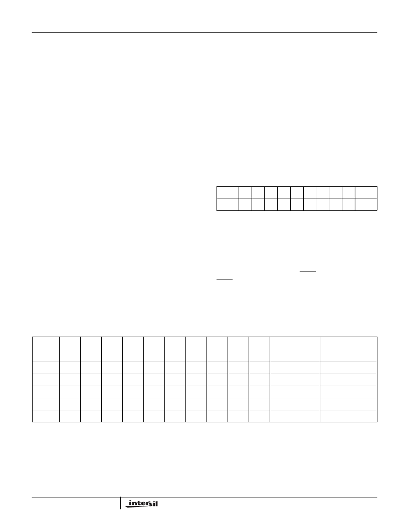
The length control inputs (LC0-10) are used to set the length
of the programmable delay ram which can vary in length
from 0 to 1279. The total length of the HSP9501 data buffer
will then be equal to the programmed value on LC0-10 plus
2. The programmed delay is established by the 11-bit integer
value of the LC0-10 inputs with LC-10 as the MSB and LC0
as the LSB.
For example,
programs a length value of 2
6
+ 2
0
= 65. The total length of
the delay will be 65 + 2 or 67 delays.
Table 1 indicates several programming values. The decimal
value placed on LC0-10 must not exceed 1279. Controlled
operation with larger values is not guaranteed.
Values on LC0-10 are latched on the CLK edge selected by
the CLKSEL control line, when LCEN is active. LC0-10 and
LCEN must meet the specified setup and hold times relative
to the selected CLK edge for proper device operation.
LC10
9
8
7
6
5
4
3
2
1
LC0
0
0
0
0
1
0
0
0
0
0
1
TABLE 1. LENGTH CONTROL PROGRAMMING EXAMPLES
LC10 2
10
LC9
2
9
LS8
2
8
LC7
2
7
LC6
2
6
LC5
2
5
LC4
2
4
LC3
2
3
LC2
2
2
LC1
2
1
LC0
2
0
PROGRAMMED
LENGTH
TOTAL
LENGTH
N
0
0
0
0
0
0
0
0
0
0
0
0
2
0
0
0
0
1
1
1
0
1
1
0
118
120
0
1
1
0
0
1
0
1
0
0
0
808
810
1
0
0
0
0
0
1
1
0
0
1
1049
1051
1
0
0
1
1
1
1
1
1
1
1
1279
1281
HSP9501
相關(guān)PDF資料 |
PDF描述 |
|---|---|
| HSP9501JC-32 | Programmable Data Buffer |
| HSR101 | |
| HSSR-8400 | 400 V/10 Ohm, General Purpose, 1 Form A, Solid State Relay |
| HT0-440N4 | Interface IC |
| HT0-740N4 | Interface IC |
相關(guān)代理商/技術(shù)參數(shù) |
參數(shù)描述 |
|---|---|
| HSP9501JC-32 | 功能描述:緩沖器和線路驅(qū)動(dòng)器 PROGRAMMABLE DATA BUFFER 44 PLCC, 32MHZ, COMM RoHS:否 制造商:Micrel 輸入線路數(shù)量:1 輸出線路數(shù)量:2 極性:Non-Inverting 電源電壓-最大:+/- 5.5 V 電源電壓-最小:+/- 2.37 V 最大工作溫度:+ 85 C 安裝風(fēng)格:SMD/SMT 封裝 / 箱體:MSOP-8 封裝:Reel |
| HSP9512CP WAF | 制造商:Harris Corporation 功能描述: |
| HSP9520 | 制造商:INTERSIL 制造商全稱:Intersil Corporation 功能描述:Multilevel Pipeline Registers |
| HSP9520 WAF | 制造商:Harris Corporation 功能描述: |
| HSP9520CP | 制造商:Rochester Electronics LLC 功能描述:- Bulk |
發(fā)布緊急采購,3分鐘左右您將得到回復(fù)。