- 您現(xiàn)在的位置:買賣IC網(wǎng) > PDF目錄371898 > HSP45256883 (Intersil Corporation) Binary Correlator PDF資料下載
參數(shù)資料
| 型號(hào): | HSP45256883 |
| 廠商: | Intersil Corporation |
| 英文描述: | Binary Correlator |
| 中文描述: | 二元相關(guān)器 |
| 文件頁數(shù): | 9/23頁 |
| 文件大小: | 154K |
| 代理商: | HSP45256883 |

9
Weight and Sum Logic
The Weight and Sum Logic provides the bit weighting and
the final correlator score from the eight stages of the
correlation array. For a 1 x 256 1-D configuration, the outputs
of each of the stages are given a weight of 1 and then added
together. In a 8 x 32 (8-bit data) configuration, the output of
each stage will be shifted so that the output data represents
an 8-bit word, with stage seven being the MSB.
The 13-bit Offset Register is loaded from the control data
bus. Its output is added to the correlation score obtained
from the correlator array. This sum then goes to the
programmable delay register data input.
When the chip is configured as dual correlators, the user has
the capability of loading two different offset values, one for
each of the two correlators.
The Programmable Delay Register sets the number of
pipeline stages between the output of the weight and sum
logic and the input of the Cascade Summer. This delay
register is used to align the correlation scores of multiple
correlators in HSP45256 cascaded configurations (see
Applications Section). The number of delays is
programmable from 1 to 16, allowing for up to 16 correlators
to be cascaded. When the HSP45256 is configured as dual
correlators, the delay must be set to 0000, which specifies a
delay of 1.
Cascade Summer
The Cascade Summer is used for cascading several
correlator chips together. The value present on this bus
represents the correlation score from the previous
HSP45256 that will be summed with the current score to
provide the final correlation score. When several correlator
chips are cascaded, the CASOUT0-12 of each correlator is
connected to the CASIN0-12 of the next correlator in the
chain. The CASIN0-12 of the first chip is tied low. The
following function represents the correlation score present
on CASOUT0-12 of each correlator:
CASOUT(n) = (W7 x CO7)(n-Delay) + (W6 x CO6)(n-Delay) +
(W5 x CO5)(n-Delay) + (W4 x CO4)(n-Delay) +
(W3 x CO3)(n-Delay) + (W2 x CO2)(n-Delay) +
(W1 x CO1)(n-Delay) + (W0 x CO0)(n-Delay) +
Offset (n-Delay) + CASIN.
where:
CO0-CO7 are the correlation score outputs out of the
correlation stages; W0-W7 is the weight given to each stage;
n-Delay represents the delay on the weighted and summed
correlation score through the Programmable Delay Register;
Offset is the value programmed into the Offset register;
CASIN is the cascade input.
Control Registers
The 3-bit address value, A0-2, is used to determine which
internal register will be loaded with the data on DCONT0-7.
The function is initiated when CLOAD is brought low, and the
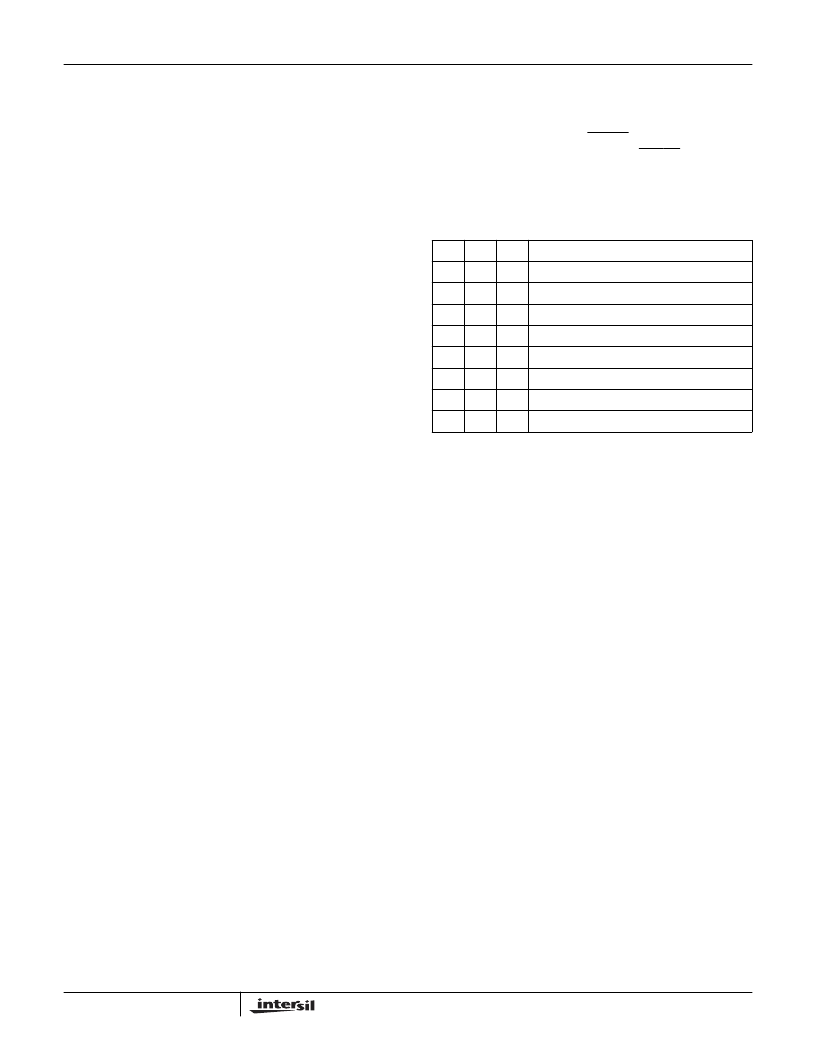
register is loaded on the rising edge of CLOAD. Table 1
indicates the function associated with each address. Tables
2 - 8 define the function of the bits in each of the control
registers.
TABLE 1. ADDRESS MAPPING
A2
A1
A0
DESTINATION
0
0
0
Mask Register
0
0
1
Configuration Register
0
1
0
Offset Register A-Most Significant Bits
0
1
1
Offset Register A-Least Significant Bits
1
0
0
Programmable Delay Register
1
0
1
Offset Register B-Most Significant Bits
1
1
0
Offset Register B-Least Significant Bits
1
1
1
Reserved
HSP45256
相關(guān)PDF資料 |
PDF描述 |
|---|---|
| HSP45256JC-25 | Binary Correlator |
| HSP45256JC-33 | Binary Correlator |
| HSP48410GC-33 | Histogrammer/Accumulating Buffer |
| HSP48410GC-40 | Histogrammer/Accumulating Buffer |
| HSP48410 | Histogrammer/Accumulating Buffer |
相關(guān)代理商/技術(shù)參數(shù) |
參數(shù)描述 |
|---|---|
| HSP45256GC-25 | 制造商:INTERSIL 制造商全稱:Intersil Corporation 功能描述:Binary Correlator |
| HSP45256GC-33 | 制造商:Rochester Electronics LLC 功能描述:- Bulk 制造商:Harris Corporation 功能描述: |
| HSP45256GM-20/883 | 制造商:Rochester Electronics LLC 功能描述:BINARY CORRELATOR 85 PGA, 20MHZ, MIL 883 - Bulk 制造商:Harris Corporation 功能描述: |
| HSP45256GM-25/883 | 制造商:INTERSIL 制造商全稱:Intersil Corporation 功能描述:Binary Correlator |
| HSP45256JC-25 | 制造商:INTERSIL 制造商全稱:Intersil Corporation 功能描述:Binary Correlator |
發(fā)布緊急采購,3分鐘左右您將得到回復(fù)。