- 您現(xiàn)在的位置:買賣IC網(wǎng) > PDF目錄67681 > HPMX-2003T10 (AGILENT TECHNOLOGIES INC) 800 MHz - 1000 MHz RF/MICROWAVE VECTOR MODULATOR PDF資料下載
參數(shù)資料
| 型號(hào): | HPMX-2003T10 |
| 廠商: | AGILENT TECHNOLOGIES INC |
| 元件分類: | 調(diào)制器/解調(diào)器 |
| 英文描述: | 800 MHz - 1000 MHz RF/MICROWAVE VECTOR MODULATOR |
| 文件頁(yè)數(shù): | 6/16頁(yè) |
| 文件大?。?/td> | 188K |
| 代理商: | HPMX-2003T10 |
第1頁(yè)第2頁(yè)第3頁(yè)第4頁(yè)第5頁(yè)當(dāng)前第6頁(yè)第7頁(yè)第8頁(yè)第9頁(yè)第10頁(yè)第11頁(yè)第12頁(yè)第13頁(yè)第14頁(yè)第15頁(yè)第16頁(yè)
14
HPMX-2003 JDC
Applications
The JDC System
JDC (Japan Digital Cellular) com-
monly refers to the Japanese digi-
tal cellular telephone system
standard. Digital cellular phones
for the Japanese market must
conform to this standard. The JDC
system is characterized by 25 kHz
channel spacing and mobile to
base transmit frequencies of 940 –
960 MHz. The primary modulation
characteristics include
π/4 DQPSK
filtering of the I and Q signals and
42 kbps transmission rate.
Critical Performance
Parameters
JDC standards require that the
telephone exhibit RMS modula-
tion error
≤12.5%. The modulated
output spectrum of the phone
must lie within a “spectral mask”
which defines maximum allow-
able radiation levels into adjacent
and alternate channels. Specifi-
cally, 50 kHz from the channel
center frequency (f0), the output
of the phone must be at least
45 dB below the peak output at f0.
100 kHz from f0, the output must
be at least 60 dB below the peak
output at f0. Refer to the JDC
specifications for more detailed
information.
HPMX-2003 Performance
The typical RMS modulation error
level of 4% makes the HPMX-2003
an excellent choice for JDC appli-
cations. The output spectrum falls
easily within the JDC spectral
mask, and the high power and
simple output configuration mean
lower components count, reduced
size and higher system efficiency.
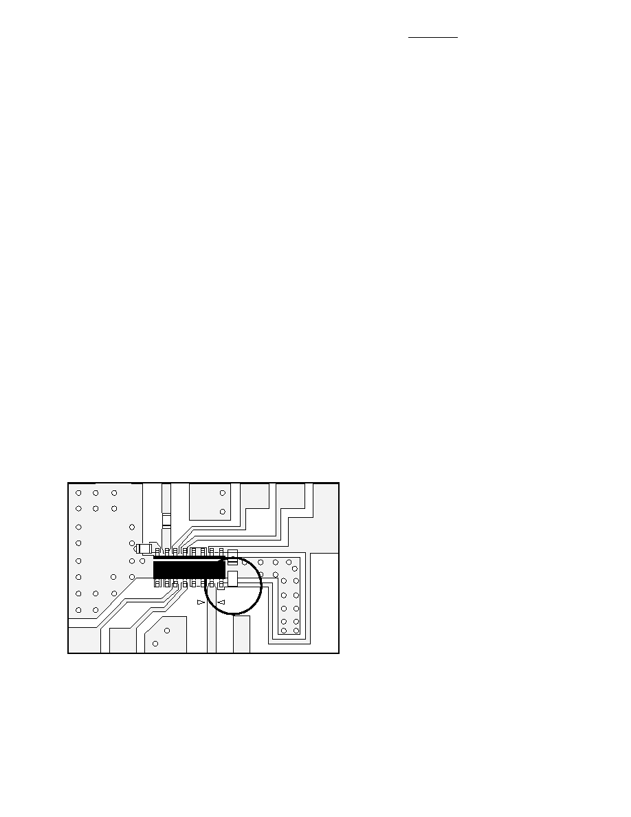
Particulars of Use
Many of the JDC application per-
formance graphs shown in this
data sheet were created using the
test board shown in figure 41,
below.
The only external components
required by this IC are four chip
capacitors. One capacitor is used
as a DC block on the input trans-
mission line. The second capaci-
tor (at pin 8) provides an AC
ground to one side of the differen-
tial LO input. The third and fourth
capacitors (at pins 1 and 16) are
for VCC bypass.
The circuit board includes an in-
ductive trace that can optionally
be used to minimize output VSWR
by placing a bypass capacitor at
various points along the inductive
line. Minimum VSWR for JDC
applications is achieved by plac-
ing the capacitor as shown in the
circle (inductance
≈ 0 nH).
The IC has an internal blocking
capacitor so the output is a simple
50
transmission line. An en-
larged scale layout of this board
can be found on the last page of
this data sheet.
Figure 41. HPMX-2003 JDC Test Board.
LO
Q
R
VCC
5 V
OUT
R
C
I
H
HPMX-2003/5
VER. 1
相關(guān)PDF資料 |
PDF描述 |
|---|---|
| HPMX-2005T10 | 25 MHz - 250 MHz RF/MICROWAVE VECTOR MODULATOR |
| HPMX-2005 | 50 MHz - 200 MHz RF/MICROWAVE VECTOR MODULATOR |
| HPMX-5001 | 1500 MHz - 2500 MHz RF/MICROWAVE UP/DOWN CONVERTER, 2 dBm OUTPUT POWER-MAX |
| HPMX-5001 | 1500 MHz - 2500 MHz RF/MICROWAVE UP/DOWN CONVERTER, 2 dBm OUTPUT POWER-MAX |
| HPMX-7102-BLK | RF/MICROWAVE DOWN CONVERTER |
相關(guān)代理商/技術(shù)參數(shù) |
參數(shù)描述 |
|---|---|
| HPMX-2005 | 制造商:Hewlett Packard Co 功能描述:25 MHz - 250 MHz RF/MICROWAVE VECTOR MODULATOR |
| HPMX-2005_1 | 制造商:HITTITE 制造商全稱:Hittite Microwave Corporation 功能描述:Silicon Bipolar RFIC 100 MHz Vector Modulator |
| HPMX-2006 | 制造商:AGILENT 制造商全稱:AGILENT 功能描述:0.8 - 2.5 GHz Upconverter/Amplifier |
| HPMX-2006-BLK | 制造商:AGILENT 制造商全稱:AGILENT 功能描述:0.8 - 2.5 GHz Upconverter/Amplifier |
| HPMX-2006-TR1 | 制造商:AGILENT 制造商全稱:AGILENT 功能描述:0.8 - 2.5 GHz Upconverter/Amplifier |
發(fā)布緊急采購(gòu),3分鐘左右您將得到回復(fù)。