- 您現(xiàn)在的位置:買賣IC網(wǎng) > PDF目錄370661 > HPC3130PBKLOW-PROFILEQUAD (Texas Instruments, Inc.) PCI HOT PLUG CONTROLLER PDF資料下載
參數(shù)資料
| 型號: | HPC3130PBKLOW-PROFILEQUAD |
| 廠商: | Texas Instruments, Inc. |
| 英文描述: | PCI HOT PLUG CONTROLLER |
| 中文描述: | 的PCI熱插拔控制器 |
| 文件頁數(shù): | 16/40頁 |
| 文件大小: | 555K |
| 代理商: | HPC3130PBKLOW-PROFILEQUAD |
第1頁第2頁第3頁第4頁第5頁第6頁第7頁第8頁第9頁第10頁第11頁第12頁第13頁第14頁第15頁當(dāng)前第16頁第17頁第18頁第19頁第20頁第21頁第22頁第23頁第24頁第25頁第26頁第27頁第28頁第29頁第30頁第31頁第32頁第33頁第34頁第35頁第36頁第37頁第38頁第39頁第40頁

HPC3130
PCI HOT PLUG CONTROLLER
SCPS029B – DECEMBER1998
16
POST OFFICE BOX 655303
DALLAS, TEXAS 75265
8–BIT
PORT
HOST/PCI
INTR
PCLK
PRST
SYSM66EN
BUSON
CBT–SW
CBT–SW
CLKON
CBT–SW
REQ64ON
SLOTREQ64
M66EN
PRSNT(1–2)
P
C
I
S
L
O
T
SLOTRST
PWRON/OFF
PERFAULT
PWRGOOD
PWR–SW
DETECT(0–1)
ATTN(0–1)
FRAME
IRDY
IDLEREQ
IDLEGNT
HPC–PCI
PCI Bus
PCI Bus Less PRST and REQ64
Motherboard
PCI Device
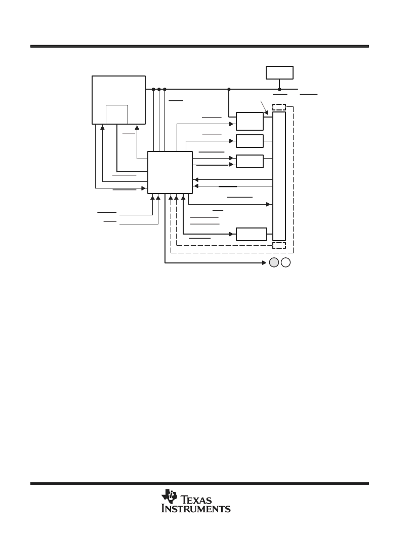
Figure 1. HPC3130 Implementation
The HPC3130 internal registers can be accessed through either a two-wire serial interface or an 8-bit generic
parallel bus (ISA-like). The above figure illustrates the 8-bit port configuration. Not shown in the diagram is the
SMODE chip input that must be wired low to indicate parallel bus interface mode. Also not shown in the diagram
is the external chip-select logic required to select the HPC3130 in ISA bus cycles.
serial interface
The internal registers can be accessed either through a two-wire serial interface or through an 8-bit generic
parallel interface. The SMODE input selects one of these modes.
The HPC3130 implements a two-pin serial slave interface with one clock signal (SCL) and one data signal
(SDA). This serial interface can operate with a serial clock frequency up to 400 kHz. Both SCL and SDA require
pullup resistors for the serial slave interface to function properly.
All data transfers are initiated by the serial bus master. The beginning of a data transfer is indicated by a START
condition (S) when the SDA line transitions to a low state while SCL is in a high state as illustrated in Figure 2.
The end of a requested data transfer is indicated by a STOP condition (P), which is the low-to-high transition
of SDA while SCL is in the high state. Data on SDA must remain stable during the high state of the SCL signal.
Changes on the SDA signal during the high state of SCL will be interpreted as control signals, that is, a START
or STOP condition.
The SCL is an input into the HPC3130 and SDA is bidirectional.
相關(guān)PDF資料 |
PDF描述 |
|---|---|
| HPC43100VHG30 | 16-Bit Microcontroller |
| HPC46003E20 | 16-Bit Microcontroller |
| HPC46003L20 | 16-Bit Microcontroller |
| HPC46003L30 | 16-Bit Microcontroller |
| HPC46003T20 | 16-Bit Microcontroller |
相關(guān)代理商/技術(shù)參數(shù) |
參數(shù)描述 |
|---|---|
| HPC3130PBM | 功能描述:外圍驅(qū)動器與原件 - PCI HOT PLUG CONTROLLER RoHS:否 制造商:PLX Technology 工作電源電壓: 最大工作溫度: 安裝風(fēng)格:SMD/SMT 封裝 / 箱體:FCBGA-1156 封裝:Tray |
| HPC3130PBMQUADFLAT | 制造商:TI 制造商全稱:Texas Instruments 功能描述:PCI HOT PLUG CONTROLLER |
| HPC3130PGE | 制造商:未知廠家 制造商全稱:未知廠家 功能描述:PCI Bus Interface/Controller |
| HPC3130PGELOW-PROFILEQUAD | 制造商:TI 制造商全稱:Texas Instruments 功能描述:PCI HOT PLUG CONTROLLER |
| HPC36003 | 制造商:NSC 制造商全稱:National Semiconductor 功能描述:High-Performance microControllers |
發(fā)布緊急采購,3分鐘左右您將得到回復(fù)。