- 您現(xiàn)在的位置:買賣IC網(wǎng) > PDF目錄60851 > HMMC-5618 6000 MHz - 20000 MHz RF/MICROWAVE WIDE BAND LOW POWER AMPLIFIER PDF資料下載
參數(shù)資料
| 型號: | HMMC-5618 |
| 元件分類: | 放大器 |
| 英文描述: | 6000 MHz - 20000 MHz RF/MICROWAVE WIDE BAND LOW POWER AMPLIFIER |
| 文件頁數(shù): | 2/6頁 |
| 文件大小: | 72K |
| 代理商: | HMMC-5618 |
2
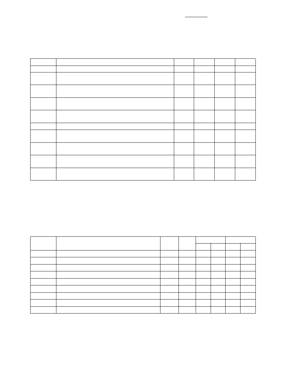
HMMC-5618 DC Specifications/Physical Properties[1]
Symbol
Parameters and Test Conditions
Units
Min.
Typ.
Max.
VD1, VD2
Drain Supply Voltage
V
3.0
5.0
5.5
ID1
Stage-One Drain Supply Current
mA
50
(VD1 = 5 V , VG1 = Open or Ground)
ID2
Stage-Two Drain Supply Current
mA
65
(VD2 = 5 V , VG2 = Open or Ground)
ID1 + ID2
Total Drain Supply Current
mA
115
140
(VD1 = VD2 = 5 V, VG1 = VG2 = Open or Ground)
VP1
Optional Input-Stage Gate Supply Pinch-off Voltage
V
-4
-2.8
(VD1 = 5 V , ID1 < 3 mA: Input Stage OFF
[2])
IG1
Gate Supply Current (Input Stage OFF[2])
mA
0.9
VP2
Optional Input-Stage Gate Supply Pinch-off Voltage
V
-7.5
-5.3
(VD2 = 5 V , ID2 < 3.6 mA: Output Stage OFF
[2])
IG2
Gate Supply Current (Output Stage OFF[2])
mA
1.7
(VD2 = 5 V , VG2 = Open or Ground)
θ
ch-bs
Thermal Resistance[3]
°C/Watt
87
(Channel-to-Backside at Tch = 150°C)
Tch
Channel Temperature[4] (TA = 100
°C, MTTF = 106 hrs,
°C
150
VD1 = VD2 = 5 V, VG1 = VG2 = Open)
Notes:
1. Backside ambient operating temperature TA = 25°C unless otherwise noted.
2. The specified FET stage is in the OFF state when biased with a gate voltage level that is sufficient to pinch off the drain
current.
3. Thermal resistance (in
°C/Watt) at a channel temperature T (°C) can be estimated using his equation:
θ(T) 87 x [T(°C)+273] / [150°C+ 273].
4. Derate MTTF by a factor of two for every 8
°C above T
ch.
HMMC-5618 RF Specifications, T
A = 25°C, VD1 = VD2 = 5 V, VG1 = VG2 = Open or Ground, ZO = 50
6– 18 GHz
5.9– 20 GHz
Symbol
Parameters and Test Conditions
Units
Typ.
Min.
Max.
Min.
Max.
Gain
Small Signal Gain
dB
14
12
11.5
Gain
Gain Flatness
dB
±0.5
S
21/ T
Temperature Coefficient of Gain
dB/
°C -0.025
(RLin)MIN
Minimum Input Return Loss
dB
12
10
9
(RL out)MIN
Minimum Output Return Loss
dB
12
10
Isolation
Reverse Isolation
dB
40
P-1dB
Output Power @ 1 dB Gain Compression
dBm
18
17
Psat
Saturated Output Power (Pin = 10 dBm)
dBm
20
18.5
NF
Noise Figure
dB
5.5
7
相關(guān)PDF資料 |
PDF描述 |
|---|---|
| HMR223.3G | 240 MHz MOBILE STATION ANTENNA, 5.1 dBi GAIN |
| HMU-PAT-FH-K103 | RF/MICROWAVE FIXED ATTENUATOR |
| HMU-PAT-FH-K109 | RF/MICROWAVE FIXED ATTENUATOR |
| HMU-PAT-FH-K110 | RF/MICROWAVE FIXED ATTENUATOR |
| HMU-PAT-FH-K101 | RF/MICROWAVE FIXED ATTENUATOR |
相關(guān)代理商/技術(shù)參數(shù) |
參數(shù)描述 |
|---|---|
| HMMC-5620 | 制造商:Agilent Technologies 功能描述:RF AMP MOD SGL GAIN AMP 20GHZ 7.5V - Gel-pak, waffle pack, wafer, diced wafer on film |
| HMMD47 | 制造商:SPRAGUE 功能描述:CAPACITOR SPRAGUE |
| HMM-HH | 制造商:Cooper Bussmann 功能描述: |
| HMMXS10 | 制造商:Sprague/Vishay 功能描述:CD310X0075 |
| HMN12816D | 制造商:HANBIT 制造商全稱:Hanbit Electronics Co.,Ltd 功能描述:Non-Volatile SRAM MODULE 2Mbit (128K x 16-Bit), 40pin-Dip, 5V |
發(fā)布緊急采購,3分鐘左右您將得到回復(fù)。