- 您現(xiàn)在的位置:買賣IC網(wǎng) > PDF目錄370635 > HM62W4100HLJP-15 (Hitachi,Ltd.) 4M High Speed SRAM (1-Mword x 4-bit) PDF資料下載
參數(shù)資料
| 型號: | HM62W4100HLJP-15 |
| 廠商: | Hitachi,Ltd. |
| 英文描述: | 4M High Speed SRAM (1-Mword x 4-bit) |
| 中文描述: | 4分高速SRAM(1 - Mword × 4位) |
| 文件頁數(shù): | 7/13頁 |
| 文件大?。?/td> | 73K |
| 代理商: | HM62W4100HLJP-15 |

HM62W4100H Series
7
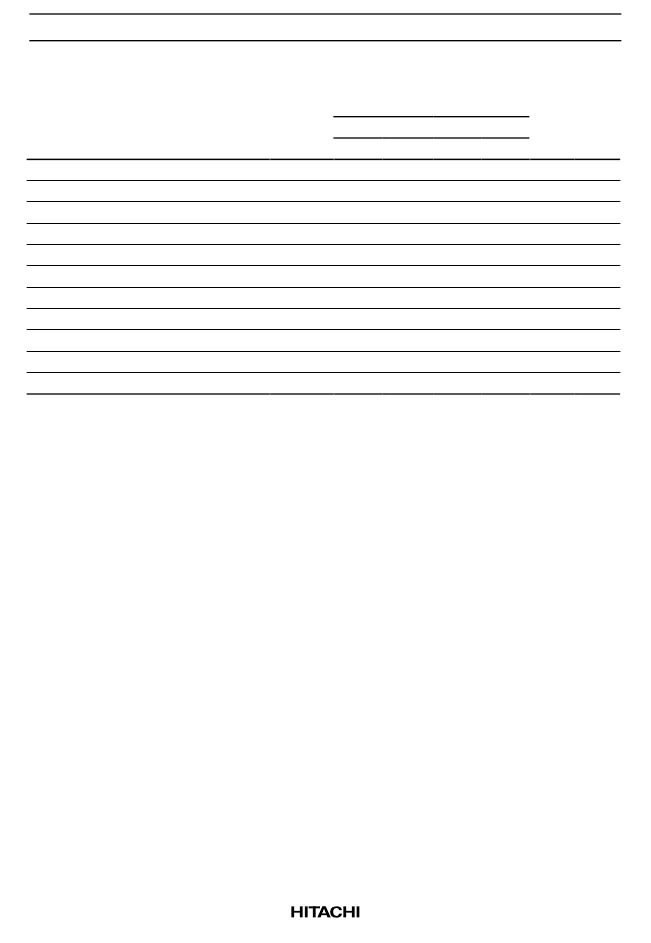
Write Cycle
HM62W4100H
-12
-15
Parameter
Symbol
Min
Max
Min
Max
Unit
Notes
Write cycle time
t
WC
t
AW
t
CW
t
WP
t
AS
t
WR
t
DW
t
DH
t
OW
t
OHZ
t
WHZ
12
—
15
—
ns
Address valid to end of write
8
—
10
—
ns
Chip select to end of write
8
—
10
—
ns
9
Write pulse width
8
—
10
—
ns
8
Address setup time
0
—
0
—
ns
6
Write recovery time
0
—
0
—
ns
7
Data to write time overlap
6
—
7
—
ns
Data hold from write time
0
—
0
—
ns
Write disable to output in low-Z
3
—
3
—
ns
1
Output disable to output in high-Z
—
6
—
7
ns
1
Write enable to output in high-Z
Note: 1. Transition is measured
±
200 mV from steady voltage with Load (B). This parameter is sampled
and not 100% tested.
2. Address should be valid prior to or coincident with
CS
transition low.
3.
WE
and/or
CS
must be high during address transition time.
4. if
CS
and
OE
are low during this period, I/O pins are in the output state. Then, the data input
signals of opposite phase to the outputs must not be applied to them.
5. If the
CS
low transition occurs simultaneously with the
WE
low transition or after the
WE
transition,
output remains a high impedance state.
6. t
AS
is measured from the latest address transition to the later of
CS
or
WE
going low.
7. t
WR
is measured from the earlier of
CS
or
WE
going high to the first address transition.
8. A write occurs during the overlap of a low
CS
and a low
WE
. A write begins at the latest transition
among
CS
going low and
WE
going low. A write ends at the earliest transition among
CS
going
high and
WE
going high. t
WP
is measured from the beginnig of write to the end of write.
9. t
CW
is measured from the later of
CS
going low to the the end of write.
—
6
—
7
ns
1
相關PDF資料 |
PDF描述 |
|---|---|
| HM62W4100H | 4M High Speed SRAM (1-Mword ×4-bit)(4M高速靜態(tài)RAM(1M字×4位)) |
| HM62W8511HJP-12 | 4M High Speed SRAM (512-kword x 8-bit) |
| HM62W8511HJP-15 | 4M High Speed SRAM (512-kword x 8-bit) |
| HM62W8511HLJP-12 | 4M High Speed SRAM (512-kword x 8-bit) |
| HM62W8511HLJP-15 | 4M High Speed SRAM (512-kword x 8-bit) |
相關代理商/技術參數(shù) |
參數(shù)描述 |
|---|---|
| HM62W8512BLFP-5 | 制造商:HITACHI 功能描述: |
| HM62W8512BLTTI7 | 制造商:Hitachi 功能描述: |
| HM-630 | 制造商:Black Box Corporation 功能描述:FACE PLATE:HM-STAINLESS |
| HM63021FP | 制造商:Panasonic Industrial Company 功能描述:IC |
| HM63021P-28 | 制造商:未知廠家 制造商全稱:未知廠家 功能描述:Field/Frame/Line Memory |
發(fā)布緊急采購,3分鐘左右您將得到回復。