- 您現(xiàn)在的位置:買(mǎi)賣(mài)IC網(wǎng) > PDF目錄299176 > HIP0045AB (HARRIS SEMICONDUCTOR) 1.75 A 8 CHANNEL, LATCH BASED PRPHL DRVR, PDSO20 PDF資料下載
參數(shù)資料
| 型號(hào): | HIP0045AB |
| 廠(chǎng)商: | HARRIS SEMICONDUCTOR |
| 元件分類(lèi): | Peripheral Driver |
| 英文描述: | 1.75 A 8 CHANNEL, LATCH BASED PRPHL DRVR, PDSO20 |
| 封裝: | PLASTIC, DSO-20 |
| 文件頁(yè)數(shù): | 8/9頁(yè) |
| 文件大?。?/td> | 87K |
| 代理商: | HIP0045AB |
8
Detecting Fault Conditions
Fault conditions may be checked as follows: SCK is always
low when CE is changing. When CE goes low, the MISO
output is taken out of the three-state mode and the Output
status information is latched into the shift register. While CE is
low, data bits in the shift register are transferred to the MISO
output on each positive SCK clock transition and data bits
present at the MOSI input are transferred into the shift register
on each negative transition of SCK. To verify Status and
Diagnostic conditions, clock in a new control byte and wait
approximately 150
s to allow the outputs to settle. Clock in
the same control byte and compare this to the data output at
the MISO pin. If there is a disparity, use Tables 5, 6 and 7 to
determine the fault or status condition. (Use Tables 1, 2, 3 and
4 to establish the ON/OFF conditions for each output).
Based on the needs of the application, a software sequence
should be programmed into the microcontroller to set the
corrective action of each fault condition.
Special Conditions for Channel 0, 1
Referring to the Detailed Block Diagram, Channel’s 0, 1 are
congured to externally provide control of the ON/OFF state.
The inputs, IN0 and IN1, are ORed with the SPI ON/OFF
control bit. In this conguration with IN0 and IN1 high, SPI
control latches Diag0 and Diag1 as status bits. When the IN0
and IN1 inputs are active, a fault condition is detected by a
comparison of IN0 and IN1 to OUT0 and OUT1 respectively
causing the Fault Detector to latch a fault bit. The resulting
Fault output is latched as diagnostic bit, Diag0 or Diag1. The
Diag0 and Diag1 outputs give the status or fault condition of
the output drivers as shown in Table 6. Fault detection is
disabled during switching/settling time.
The Diag0 and Diag1 bits from Channel 0 and 1 respectively
indicate a fault when the FAULT BIT is Low, given IN1 and
IN0 control. Otherwise Diag0 and Diag1 are status bits when
controlled by the SPI input. Note that the SPI Bit, given in
Tables 1 and 2 overrides the ON state control from IN0
and IN1.
TABLE 5. DIAGNOSTIC FAILURE REGISTER STRUCTURE
Diag1
Diag3
Diag5
Diag7
Diag0
Diag2
Diag4
Diag6
(D7O)
(D6O)
(D5O)
(D4O)
(D3O)
(D2O)
(D1O)
(D0O)
MSB
LSB
NOTE:
10. The Diagnostic Failure Register bits Diag0 -7 have the same
order as the Control Register bits Q0 - 7 as defined in Table 4.
Data bits D0O - D7O give the MISO SPI serial output flow
sequence.
TABLE 6. DEFINITION OF Diag0, 1 FAULT BITS FOR OUT0,
1 IN PARALLEL-CONTROLLED MODE
OUTPUT
STATE
VREF
STATUS
FAULT
BIT
FAULT
MODE
OFF
>VREF
H
No Fault
OFF
<VREF
L
Open Load or GND Short
ON
<VREF
H
No Fault
ON
>VREF
L
Short to VBATT
TABLE 7. DEFINITION OF Diag0-7 STATUS BITS FOR OUT0-7
OUTPUT
STATE
VREF
STATUS
BIT
FAULT
MODE
OFF
>VREF
H
No Fault
OFF
<VREF
L
Open Load or GND Short
ON
<VREF
L
No Fault
ON
>VREF
H
Short to VBATT (Chan. 0-7);
or Over-Temperature Fault
(Chan. 6, 7)
NOTES:
11. For Channel 0 (Diag0) and Channel 1 (Diag1):
Fault Bit High = No Fault; Fault Bit Low = Fault Occurred.
12. VREF is the threshold reference level for detecting an Open Load.
Refer to the Electrical Specification for the VREF voltage level.
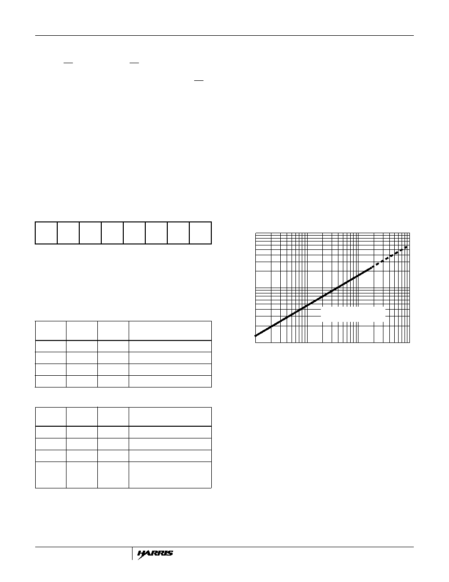
0.1
1
10
100
10
100
1000
TIME (ms)
ENERGY
(mJ)
SAFE OPERATING AREA
BELOW LINE
FIGURE 4. MAXIMUM SINGLE PULSE ENERGY SAFE
OPERATING AREA FOR EACH CLAMPED
OUTPUT DRIVER, TA = 25
oC
HIP0045
相關(guān)PDF資料 |
PDF描述 |
|---|---|
| HIP0050IB | 0.3 A BUF OR INV BASED PRPHL DRVR, PDSO24 |
| HIP1030AS | 1.6 A BUF OR INV BASED PRPHL DRVR, PSFM5 |
| HK10051N2S | 1 ELEMENT, 0.0012 uH, FERRITE-CORE, GENERAL PURPOSE INDUCTOR, SMD |
| HK1005R10K | 1 ELEMENT, 0.1 uH, FERRITE-CORE, GENERAL PURPOSE INDUCTOR, SMD |
| HK100582NK | 1 ELEMENT, 0.082 uH, FERRITE-CORE, GENERAL PURPOSE INDUCTOR, SMD |
相關(guān)代理商/技術(shù)參數(shù) |
參數(shù)描述 |
|---|---|
| HIP0045ABT | 制造商:Rochester Electronics LLC 功能描述:- Tape and Reel |
| HIP0050 | 制造商:INTERSIL 制造商全稱(chēng):Intersil Corporation 功能描述:0.3A/50V Octal Low Side Power Driver with Serial Bus Control and Over-Current Fault Flag |
| HIP0050IB | 制造商:Rochester Electronics LLC 功能描述:- Bulk |
| HIP0050IB96 | 制造商:Rochester Electronics LLC 功能描述:- Bulk |
| HIP0050IB96S2300 | 制造商:Rochester Electronics LLC 功能描述:- Bulk |
發(fā)布緊急采購(gòu),3分鐘左右您將得到回復(fù)。