- 您現(xiàn)在的位置:買賣IC網(wǎng) > PDF目錄384414 > HI-6010JF (HOLT INTEGRATED CIRCUITS INC) ARINC 429 TRANSMITTER/RECEIVER FOR 8 BIT BUS PDF資料下載
參數(shù)資料
| 型號: | HI-6010JF |
| 廠商: | HOLT INTEGRATED CIRCUITS INC |
| 元件分類: | 微控制器/微處理器 |
| 英文描述: | ARINC 429 TRANSMITTER/RECEIVER FOR 8 BIT BUS |
| 中文描述: | 1 CHANNEL(S), SERIAL COMM CONTROLLER, PQCC28 |
| 封裝: | ROHS COMPLIANT, PLASTIC, LCC-28 |
| 文件頁數(shù): | 3/12頁 |
| 文件大小: | 101K |
| 代理商: | HI-6010JF |
COMMUNICATING WITH THE CONTROL AND
STATUS REGISTERS
LABELRECOGNITIONOPTION
LOADING LABELS
READING LABELS
Pin 27, C/ , must be high to read the status register or write
the control register.
Reading the status register resets
errors. Thereisnoprovisiontoreadthecontrolregister.
Pin5mustbehighiflabelrecognitionisselectedineitherthe
8 or 32 bit modes and all eight label buffers must be written
usingredundantlabels,ifnecessary.
Thechipcomparestheincominglabeltothestoredlabels. If
a match is found, the data is processed. If a match is not
found,noindicatorsofreceivingARINCdataarepresented.
AfterthewritethatchangesCR7from0to1,thenext8writes
of data (C/
is a zero for data) will load the label registers.
Labels must be loaded whenever pin 5 goes from low to
high.
After the write that changes CR1 from 0 to 1, the next 8 data
readsarelabels.
D
D
PIN 6 - MR
When MR is a 1, the control word is set to 0X10 0101 (CR7 -
CR0).
For the receiver this sets up 8 bit mode with the
receiver and parity enabled. MR also initializes the registers
and logic. The first ARINC reception will only occur
wordgap.
IN8 - RXRDY
In 8 bit mode, this pin goes high whenever 8 bits are received
withouterror. In32bitmode,thispingoeshighafterall32bits
are received with no error. This flag may be inhibited for one
ARINC word if CR3 is programmed to 1. This flag is also
inhibitedinlabelrecognitioniftheincomingARINClabeldoes
notmatchoneofthestored8labels.
PIN12 - RXC
This pin must have a clock applied that is 4X the desired
receivefrequency.
PIN13 - FCR
In 8 bit mode, this pin flags the first character (byte) received.
In 32 bit mode, this pin goes high for a valid 32 bit word. The
pinisnotaffectedbyCR3programming.
a
after
P
USING THE RECEIVER (cont.)
receiver is not programmable to the 32 bit "extended buffer"
mode nor to the label recognition mode.
receiver:
Affecting the
PIN14 - RXD0andPIN16 - RXD1
These pins must be 5 volt logic levels.
translator between the ARINC bus and these inputs.
Typically a receiver chip, such as the HI-8482orHI-8588
is inserted between the ARINC bus and the logic chips.
RXD0 is looking for a high level for zero inputs and RXD1 is
looking for a high level for one inputs. When both inputs are
lowthisisreferredtoastheNullstate.
There must be a
By writing to the Control Register and reading the Status
Register the controlling processor can operate the receiver
without hardware interrupts.
combination with the wiring of pin 5 was explained above.
The Status Register bits pertaining to the receiver are
explainedbelow:
The Control Register in
SOFTWARE CONTROL OF THE RECEIVER
* CR3 will be automatically reset to 0 after being programmed
to a 1 at the completion of an ARINC word reception. This
allowsasoftwarelabelrecognitiondifferentfromtheautomatic
optionavailable.
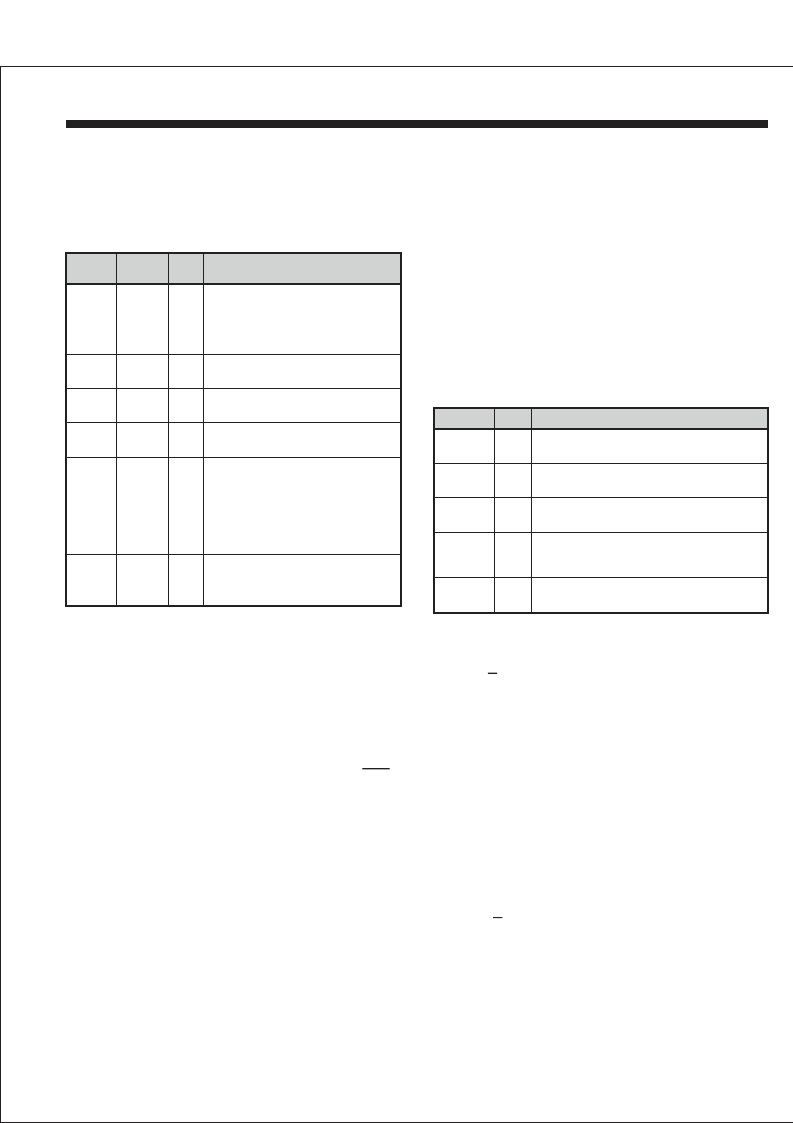
CONTROL PROGRAM PIN 5
BIT NAME
VALUE
VALUE
OPERATION
CR1
X
0
1
0
1
1
No action
No action
Next 8 data read cycles will read
stored labels. One time only sequence
on each transiton of CR1 to a 1.
CR2
0
1
X
X
Receiver is disabled
Receiver is enabled
CR3*
0
1
X
X
RXRDY goes high normally
Blocks RXRDY for one ARINC word
CR4
0
1
X
X
Self test disabled
Self test enabled
CR5
0
0
No parity errors enabled and 32nd
bit is data
Parity error flag enabled
32 bit "extended mode" enabled and
parity enabled.
8 bit "one byte at a time" mode and
parity enabled.
1
0
0
1
1
1
CR7
X
0
1
0
1
1
Label recognition not programmable
Label recognition disabled
Label recognition enabled
SR1
0
1
No receiver data
Receiver data ready
SR3
0
1
No parity error
Parity error - Parity was even
SR4
0
1
Receiver data not overwritten
Receiver data was overwritten
SR5
0
1
Receiver data received without framing error
Framing error - Did not receive exactly 32
good bits
SR6
0
1
Did not receive first byte
Received first byte - Same flag as pin 13
STATUS BIT VALUE
MEANING
HI-6010
HOLT INTEGRATED CIRCUITS
3
相關(guān)PDF資料 |
PDF描述 |
|---|---|
| HI-6010JTF | ARINC 429 TRANSMITTER/RECEIVER FOR 8 BIT BUS |
| HI-6110 | MIL-STD-1553 / MIL-STD-1760 BC / RT / MT Message Processor |
| HI-6110PQI | MIL-STD-1553 / MIL-STD-1760 BC / RT / MT Message Processor |
| HI-6110PQIF | MIL-STD-1553 / MIL-STD-1760 BC / RT / MT Message Processor |
| HI-6110PQM | MIL-STD-1553 / MIL-STD-1760 BC / RT / MT Message Processor |
相關(guān)代理商/技術(shù)參數(shù) |
參數(shù)描述 |
|---|---|
| HI-6010JT | 制造商:HOLTIC 制造商全稱:Holt Integrated Circuits 功能描述:ARINC 429 TRANSMITTER/RECEIVER FOR 8 BIT BUS |
| HI-6010JTF | 制造商:HOLTIC 制造商全稱:Holt Integrated Circuits 功能描述:ARINC 429 TRANSMITTER/RECEIVER FOR 8 BIT BUS |
| HI-6011 | 制造商:HOLTIC 制造商全稱:Holt Integrated Circuits 功能描述:ARINC 429 Transmitter / Dual Receiver for 8-Bit Bus |
| HI-6011CDT | 制造商:HOLTIC 制造商全稱:Holt Integrated Circuits 功能描述:ARINC 429 Transmitter / Dual Receiver for 8-Bit Bus |
| HI6-0201-5 | 功能描述:模擬開關(guān) IC Quad SPST CMOS Analog Switch RoHS:否 制造商:Texas Instruments 開關(guān)數(shù)量:2 開關(guān)配置:SPDT 開啟電阻(最大值):0.1 Ohms 切換電壓(最大): 開啟時間(最大值): 關(guān)閉時間(最大值): 工作電源電壓:2.7 V to 4.5 V 最大工作溫度:+ 85 C 安裝風格:SMD/SMT 封裝 / 箱體:DSBGA-16 |
發(fā)布緊急采購,3分鐘左右您將得到回復。