- 您現(xiàn)在的位置:買賣IC網(wǎng) > PDF目錄371807 > HFA3861AIN96 (INTERSIL CORP) Circular Connector; No. of Contacts:21; Series:MS27473; Body Material:Aluminum; Connecting Termination:Crimp; Connector Shell Size:22; Circular Contact Gender:Socket; Circular Shell Style:Straight Plug; Insert Arrangement:22-21 RoHS Compliant: No PDF資料下載
參數(shù)資料
| 型號: | HFA3861AIN96 |
| 廠商: | INTERSIL CORP |
| 元件分類: | 無繩電話/電話 |
| 英文描述: | Circular Connector; No. of Contacts:21; Series:MS27473; Body Material:Aluminum; Connecting Termination:Crimp; Connector Shell Size:22; Circular Contact Gender:Socket; Circular Shell Style:Straight Plug; Insert Arrangement:22-21 RoHS Compliant: No |
| 中文描述: | TELECOM, CELLULAR, BASEBAND CIRCUIT, PQFP64 |
| 封裝: | 10 X 10 MM, PLASTIC, MS-026ACD, TQFP-64 |
| 文件頁數(shù): | 33/37頁 |
| 文件大小: | 440K |
| 代理商: | HFA3861AIN96 |
第1頁第2頁第3頁第4頁第5頁第6頁第7頁第8頁第9頁第10頁第11頁第12頁第13頁第14頁第15頁第16頁第17頁第18頁第19頁第20頁第21頁第22頁第23頁第24頁第25頁第26頁第27頁第28頁第29頁第30頁第31頁第32頁當(dāng)前第33頁第34頁第35頁第36頁第37頁
33
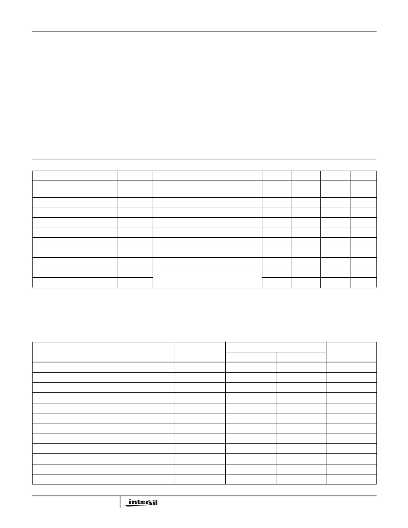
Absolute Maximum Ratings
Thermal Information
Supply Voltage. . . . . . . . . . . . . . . . . . . . . . . . . . . . . . . . . . . . . . 4.0V
Input, Output or I/O Voltage. . . . . . . . . . . .GND -0.5V to V
CC
+0.5V
ESD Classification . . . . . . . . . . . . . . . . . . . . . . . . . . . . . . . . .Class 2
Operating Conditions
Voltage Range. . . . . . . . . . . . . . . . . . . . . . . . . . . .+2.70V to +3.60V
Temperature Range. . . . . . . . . . . . . . . . . . . . . . . . . . -40
o
C to 85
o
C
Thermal Resistance (Typical, Note 4)
TQFP Package. . . . . . . . . . . . . . . . . . . . . . . . . . . . .
Maximum Storage Temperature Range . . . . . . . . . -65
o
C to 150
o
C
Maximum Junction Temperature . . . . . . . . . . . . . . . . . . . . . . .150
o
C
Maximum Lead Temperature (Soldering 10s). . . . . . . . . . . . .300
o
C
(Lead Tips Only)
θ
JA
(
o
C/W)
60
Die Characteristics
Gate Count . . . . . . . . . . . . . . . . . . . . . . . . . . . . . . . . 175,000 Gates
CAUTION: Stresses above those listed in “Absolute Maximum Ratings” may cause permanent damage to the device. This is a stress only rating and operation of the
device at these or any other conditions above those indicated in the operational sections of this specification is not implied.
NOTE:
4.
θ
JA
is measured with the component mounted on an evaluation PC board in free air.
Electrical Specifications
V
CC
= 3.0V to 3.3V
±
10%, T
A
= -40
o
C to 85
o
C
PARAMETER
SYMBOL
TEST CONDITIONS
MIN
TYP
MAX
UNITS
Power Supply Current
I
CCOP
V
CC
= 3.6V, CLK Frequency 44MHz
(Notes 5, 6, 7)
-
50
60
mA
Standby Power Supply Current
I
CCSB
I
I
I
O
V
IH
V
IL
V
OH
V
OL
C
IN
C
OUT
V
CC
= Max, Outputs Not Loaded
V
CC
= Max, Input = 0V or V
CC
V
CC
= Max, Input = 0V or V
CC
V
CC
= Max, Min
V
CC
= Min, Max
I
OH
= -1mA, V
CC
= Min
I
OL
= 2mA, V
CC
= Min
CLK Frequency 1MHz. All measurements
referenced to GND. T
A
= 25
o
C, Note 6
-
0.5
1
mA
Input Leakage Current
-10
1
10
μ
A
Output Leakage Current
-10
1
10
μ
A
Logical One Input Voltage
0.7 V
CC
-
-
-
V
Logical Zero Input Voltage
-
V
CC
/3
-
V
Logical One Output Voltage
V
CC
-0.2
-
-
V
Logical Zero Output Voltage
0.1
0.2
V
Input Capacitance
-
5
10
pF
Output Capacitance
-
5
10
pF
NOTES:
5. Output load 40pF.
6. Not tested, but characterized at initial design and at major process/design changes.
7. User must allow for peak supply current of 100mA that lasts for 20
μ
s when cir estimate is run, once per packet.
AC Electrical Specifications
V
CC
= 3.0V to 3.3V
±
10%, T
A
= -40
o
C to 85
o
C (Note 8)
PARAMETER
SYMBOL
MCLK = 44MHz
UNITS
MIN
MAX
MCLK Period
t
CP
22.5
-
ns
MCLK Duty Cycle
40/60
60/40
%
Rise/Fall (All Outputs)
-
10
ns (Notes 9, 10)
TX_PE to I
OUT
/Q
OUT
(1st Valid Chip)
t
D1
2.18
2.3
μ
s (Notes 9, 11)
TX_PE Inactive Width
t
TLP
2.22
-
μ
s (Notes 9, 12)
TX_CLK Width Hi or Low
t
TCD
40
-
ns
TX_RDY Active to 1st TX_CLK Hi
t
RC
260
-
ns
Setup TXD to TX_CLK Hi
t
TDS
30
-
ns
Hold TXD to TX_CLK Hi
t
TDH
0
-
ns
TX_CLK to TX_PE Inactive (1Mbps)
t
PEH
0
965
ns (Notes 9, 20)
TX_CLK to TX_PE Inactive (2Mbps)
t
PEH
0
420
ns (Notes 9, 20)
TX_CLK to TX_PE Inactive (5.5Mbps)
t
PEH
0
160
ns (Notes 9, 20)
HFA3861A
相關(guān)PDF資料 |
PDF描述 |
|---|---|
| HFA3861AIN | 288 MACROCELL 3.3 VOLT ISP CPLD |
| HFA3863IN | Direct Sequence Spread Spectrum Baseband Processor |
| HFA3863IN96 | Direct Sequence Spread Spectrum Baseband Processor |
| HFA3863 | Direct Sequence Spread Spectrum Baseband Processor(直接序列擴(kuò)譜基帶處理器) |
| HFA3983IV96 | 2.4GHz Power Amplifier and Detector |
相關(guān)代理商/技術(shù)參數(shù) |
參數(shù)描述 |
|---|---|
| HFA3861B | 制造商:INTERSIL 制造商全稱:Intersil Corporation 功能描述:Direct Sequence Spread Spectrum Baseband Processor |
| HFA3861BIN | 制造商:INTERSIL 制造商全稱:Intersil Corporation 功能描述:Direct Sequence Spread Spectrum Baseband Processor |
| HFA3861BIN96 | 制造商:INTERSIL 制造商全稱:Intersil Corporation 功能描述:Direct Sequence Spread Spectrum Baseband Processor |
| HFA3861IV | 制造商:INTERSIL 制造商全稱:Intersil Corporation 功能描述:Direct Sequence Spread Spectrum Baseband Processor |
| HFA3861IV96 | 制造商:INTERSIL 制造商全稱:Intersil Corporation 功能描述:Direct Sequence Spread Spectrum Baseband Processor |
發(fā)布緊急采購,3分鐘左右您將得到回復(fù)。