- 您現(xiàn)在的位置:買賣IC網(wǎng) > PDF目錄370464 > HD61602 (Hitachi,Ltd.) Segment Type LCD Driver(段類型LCD驅(qū)動器) PDF資料下載
參數(shù)資料
| 型號: | HD61602 |
| 廠商: | Hitachi,Ltd. |
| 英文描述: | Segment Type LCD Driver(段類型LCD驅(qū)動器) |
| 中文描述: | 段類型LCD驅(qū)動器(段類型液晶驅(qū)動器) |
| 文件頁數(shù): | 23/37頁 |
| 文件大小: | 229K |
| 代理商: | HD61602 |
第1頁第2頁第3頁第4頁第5頁第6頁第7頁第8頁第9頁第10頁第11頁第12頁第13頁第14頁第15頁第16頁第17頁第18頁第19頁第20頁第21頁第22頁當(dāng)前第23頁第24頁第25頁第26頁第27頁第28頁第29頁第30頁第31頁第32頁第33頁第34頁第35頁第36頁第37頁
HD61602/HD61603
1252
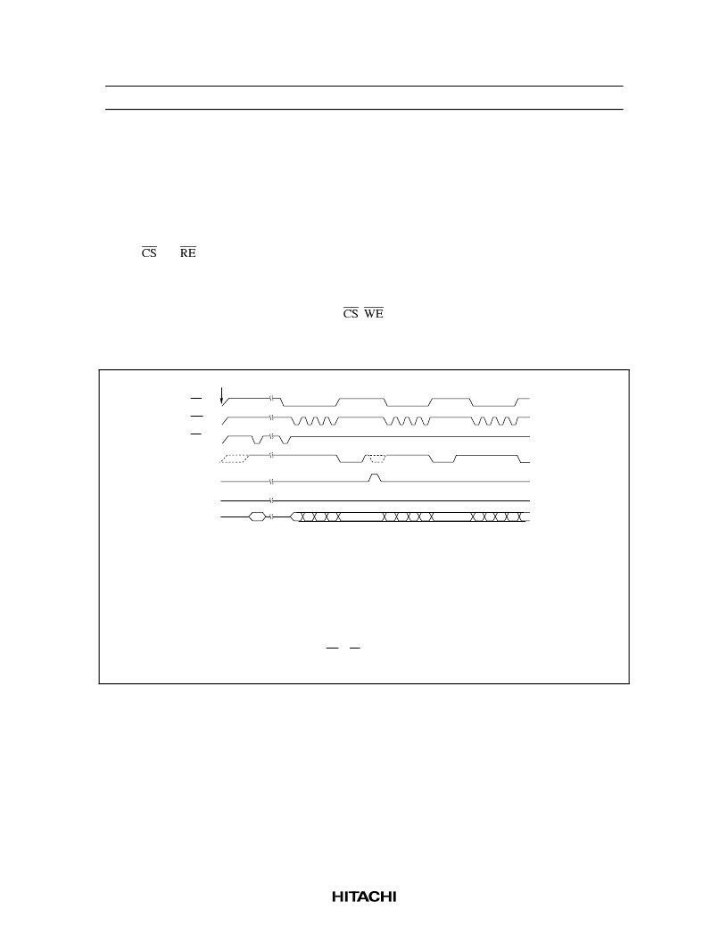
How to Input HD61603 Data
Input data is composed of 4 bits
×
4. Take care that data transfer is not interrupted, because the first 4-bit
data to the fourth 4-bit data are distinguished from each other by the sequence only.
If data transfer is interrupted, or at power on, the following two methods can be used to reset the count of
the number of data (count of the first 4-bit data to the fourth 4-bit data):
1. Set
&6
and
5(
low.
2. Input 4 or more “1-byte instruction” data (4-bit data) in which bit 3 and 2 are 1 (display data may
change).
The data input method via data input terminals (
&6
,
:(
, D0 to D3) is similar to that of static RAM such
as HM6116. An access of the LSI can be made through the same bus line as ROM and RAM. When
output ports of a microprocessor are used for an access, refer to the timing specifications and Figure 17.
Power on
CS
WE
RE
READY
SYNC
SB
D0–D3
*
6
*
6
*
1
*
4
*
5
*
3
*
2
*
5
*
5
Mode setting data
Mode setting data
Display data
1st 2nd 3rd
4th
1st
2nd 3rd
4th
1st 2nd 3rd
4th
Notes: 1.
2.
3.
4.
5.
6.
7.
READY output is indefinite during 12 clocks after the oscillation start at power on (clock:
OSC2 clock).
High pulse should be applied to SYNC terminal when using two or more chips
synchronously.
In the mode in which READY is always available, READY output is in definite while SYNC
is high.
Reset the 4-bit data counter after power on.
READY output period is within 3.5 clocks in the mode setting operation and bit
manipulation or within 10.5 clocks when the display data (8 bits) is updated.
Connect a pull-up resister if WE or RE may be floating.
It is not always necessary to follow this example.
Figure 17 Example of Data Transfer Sequence
相關(guān)PDF資料 |
PDF描述 |
|---|---|
| HD61604 | Segment Type LCD Driver(段類型LCD驅(qū)動器) |
| HD61605 | Segment Type LCD Driver(段類型LCD驅(qū)動器) |
| HD61830A00H | LCDC (LCD Timing Controller) |
| HD61830 | LCDC (LCD Timing Controller) |
| HD61830B | LCDC (LCD Timing Controller) |
相關(guān)代理商/技術(shù)參數(shù) |
參數(shù)描述 |
|---|---|
| HD61602R | 制造商:HITACHI 制造商全稱:Hitachi Semiconductor 功能描述:SEGMENT TYPE LCD DRIVER |
| HD61602RH | 制造商:HITACHI 制造商全稱:Hitachi Semiconductor 功能描述:SEGMENT TYPE LCD DRIVER |
| HD61603 | 制造商:HITACHI 制造商全稱:Hitachi Semiconductor 功能描述:SEGMENT TYPE LCD DRIVER |
| HD61603R | 制造商:HITACHI 制造商全稱:Hitachi Semiconductor 功能描述:SEGMENT TYPE LCD DRIVER |
| HD61604 | 制造商:未知廠家 制造商全稱:未知廠家 功能描述:LCD Display Driver |
發(fā)布緊急采購,3分鐘左右您將得到回復(fù)。