- 您現(xiàn)在的位置:買賣IC網(wǎng) > PDF目錄371779 > HCPL-J312 2.0 Amp Output Current IGBT Gate Drive Optocoupler(2.0 Amp 輸出電流 IGBT門驅(qū)動(dòng)耦合器) PDF資料下載
參數(shù)資料
| 型號(hào): | HCPL-J312 |
| 英文描述: | 2.0 Amp Output Current IGBT Gate Drive Optocoupler(2.0 Amp 輸出電流 IGBT門驅(qū)動(dòng)耦合器) |
| 中文描述: | 2.0安培輸出電流IGBT柵極驅(qū)動(dòng)光電耦合器(2.0安培輸出電流IGBT的門驅(qū)動(dòng)耦合器) |
| 文件頁數(shù): | 19/24頁 |
| 文件大?。?/td> | 310K |
| 代理商: | HCPL-J312 |
19
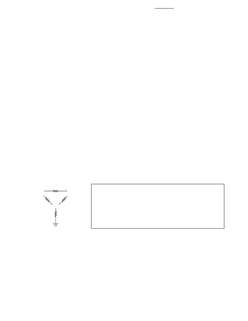
Thermal Model
(Discussion applies to
HCPL-3120, HCPL-J312
and HCNW3120)
The steady state thermal model
for the HCPL-3120 is shown in
Figure 28. The thermal resistance
values given in this model can be
used to calculate the tempera-
tures at each node for a given
operating condition. As shown by
the model, all heat generated
flows through
θ
CA
which raises
the case temperature T
C
accordingly. The value of
θ
CA
depends on the conditions of the
board design and is, therefore,
determined by the designer. The
value of
θ
CA
= 83
°
C/W was
obtained from thermal measure-
ments using a 2.5 x 2.5 inch PC
board, with small traces (no
ground plane), a single HCPL-
3120 soldered into the center of
the board and still air. The
absolute maximum power
dissipation derating specifications
assume a
θ
CA
value of 83
°
C/W.
From the thermal mode in Figure
28 the LED and detector IC
junction temperatures can be
expressed as:
T
JE
= P
E
(
θ
LC
||(
θ
LD
+
θ
DC
) +
θ
CA
)
*
θ
DC
+
T
A
θ
LC
+
θ
DC
+
θ
LD
+ P
D
(
––––––––––––––––
+
θ
CA
)
θ
LC
+
θ
DC
+
θ
LD
T
JD
=
P
E
(
––––––––––––––– +
θ
CA
)
+
P
D
(
θ
DC
||(
θ
LD
+
θ
LC
) +
θ
CA
) +
T
A
Inserting the values for
θ
LC
and
θ
DC
shown in Figure 28 gives:
T
JE
= P
E
(256
°
C/W +
θ
CA
)
+ P
D
(57
°
C/W +
θ
CA
) +
T
A
T
JD
= P
E
(57
°
C/W +
θ
CA
)
+ P
D
(111
°
C/W +
θ
CA
) +
T
A
For example, given P
E
= 45 mW,
P
O
= 250 mW, T
A
= 70
°
C and
θ
CA
= 83
°
C/W:
T
JE
= P
E
339
°
C/W + P
D
140
°
C/W +
T
A
= 45 mW
339
°
C/W + 250 m
W
140
°
C/W + 70
°
C = 120
°
C
T
JD
= P
E
140
°
C/W + P
D
194
°
C/W +
T
A
= 45 mW
140C/W + 250 m
W
194
°
C/W + 70
°
C = 125
°
C
T
JE
and T
JD
should be limited to
125
°
C based on the board layout
and part placement (
θ
CA
) specific
to the application.
T
JE
= LED junction temperature
T
JD
= detector IC junction temperature
T
C
= case temperature measured at the center of the package bottom
θ
LC
= LED-to-case thermal resistance
θ
LD
= LED-to-detector thermal resistance
θ
DC
= detector-to-case thermal resistance
θ
CA
= case-to-ambient thermal resistance
θ
CA
will depend on the board design and the placement of the part.
Figure 28. Thermal Model.
θ
LD
= 442 °C/W
T
JE
T
JD
θ
LC
= 467 °C/W
θ
DC
= 126 °C/W
θ
CA
= 83 °C/W*
T
C
T
A
相關(guān)PDF資料 |
PDF描述 |
|---|---|
| HCPL-3120 | 2.0 Amp Output Current IGBT Gate Drive Optocoupler(2.0 Amp 輸出電流 IGBT門驅(qū)動(dòng)耦合器) |
| HCPL0201 | Receptacle With No Tail |
| HCPL0211 | LOGIC-GATE-OUTPUT OPTOCOUPLER |
| HCPL1730 | Optoelectronic |
| HCPL1731 | Optoelectronic |
相關(guān)代理商/技術(shù)參數(shù) |
參數(shù)描述 |
|---|---|
| HCPL-J312#300 | 功能描述:邏輯輸出光電耦合器 2.0A IGBT Gate Drive RoHS:否 制造商:Fairchild Semiconductor 絕緣電壓:4243 Vrms 輸出類型:Push-Pull 最大傳播延遲時(shí)間:500 ns 最大正向二極管電壓: 最大反向二極管電壓: 最大正向二極管電流: 最大連續(xù)輸出電流:2.5 A 最大功率耗散:100 mW 最大工作溫度:+ 100 C 最小工作溫度:- 40 C 封裝 / 箱體:SO-16 封裝:Tube |
| HCPL-J312#500 | 功能描述:邏輯輸出光電耦合器 2.0A IGBT Gate Drive RoHS:否 制造商:Fairchild Semiconductor 絕緣電壓:4243 Vrms 輸出類型:Push-Pull 最大傳播延遲時(shí)間:500 ns 最大正向二極管電壓: 最大反向二極管電壓: 最大正向二極管電流: 最大連續(xù)輸出電流:2.5 A 最大功率耗散:100 mW 最大工作溫度:+ 100 C 最小工作溫度:- 40 C 封裝 / 箱體:SO-16 封裝:Tube |
| HCPL-J312-000E | 功能描述:邏輯輸出光電耦合器 2.0A IGBT Gate Drive RoHS:否 制造商:Fairchild Semiconductor 絕緣電壓:4243 Vrms 輸出類型:Push-Pull 最大傳播延遲時(shí)間:500 ns 最大正向二極管電壓: 最大反向二極管電壓: 最大正向二極管電流: 最大連續(xù)輸出電流:2.5 A 最大功率耗散:100 mW 最大工作溫度:+ 100 C 最小工作溫度:- 40 C 封裝 / 箱體:SO-16 封裝:Tube |
| HCPL-J312-300E | 功能描述:邏輯輸出光電耦合器 2.0A IGBT Gate Drive RoHS:否 制造商:Fairchild Semiconductor 絕緣電壓:4243 Vrms 輸出類型:Push-Pull 最大傳播延遲時(shí)間:500 ns 最大正向二極管電壓: 最大反向二極管電壓: 最大正向二極管電流: 最大連續(xù)輸出電流:2.5 A 最大功率耗散:100 mW 最大工作溫度:+ 100 C 最小工作溫度:- 40 C 封裝 / 箱體:SO-16 封裝:Tube |
| HCPL-J312-500E | 功能描述:邏輯輸出光電耦合器 2.0A IGBT Gate Drive RoHS:否 制造商:Fairchild Semiconductor 絕緣電壓:4243 Vrms 輸出類型:Push-Pull 最大傳播延遲時(shí)間:500 ns 最大正向二極管電壓: 最大反向二極管電壓: 最大正向二極管電流: 最大連續(xù)輸出電流:2.5 A 最大功率耗散:100 mW 最大工作溫度:+ 100 C 最小工作溫度:- 40 C 封裝 / 箱體:SO-16 封裝:Tube |
發(fā)布緊急采購,3分鐘左右您將得到回復(fù)。