- 您現(xiàn)在的位置:買賣IC網(wǎng) > PDF目錄67593 > FW250H1 (LINEAGE POWER LLC) DC-DC REG PWR SUPPLY MODULE PDF資料下載
參數(shù)資料
| 型號: | FW250H1 |
| 廠商: | LINEAGE POWER LLC |
| 元件分類: | 電源模塊 |
| 英文描述: | DC-DC REG PWR SUPPLY MODULE |
| 文件頁數(shù): | 3/20頁 |
| 文件大?。?/td> | 839K |
| 代理商: | FW250H1 |
Lineage Power
11
Data Sheet
April 2008
36 Vdc to 75 Vdc Input, 24 Vdc Output; 250 W to 300 W
FW250H1 and FW300H1 Power Modules; dc-dc Converters:
Feature Descriptions (continued)
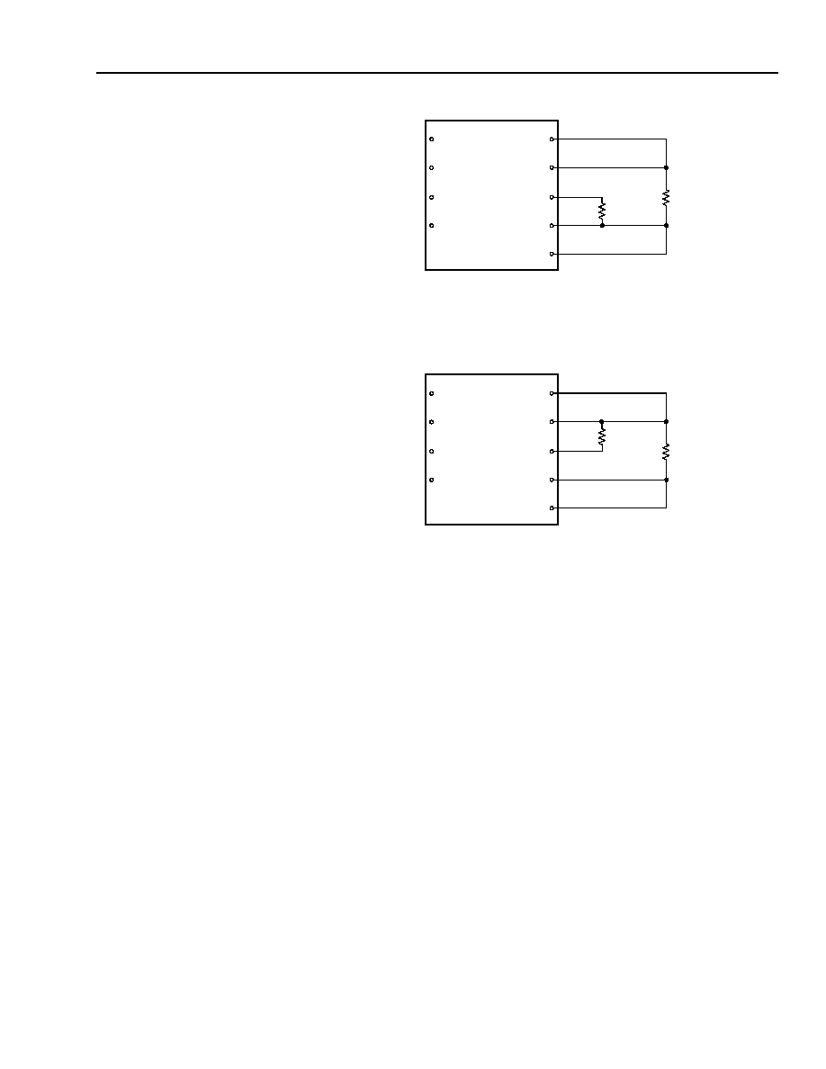
Output Voltage Set-Point Adjustment
(Trim)
Output voltage trim allows the user to increase or
decrease the output voltage set point of a module. This
is accomplished by connecting an external resistor
between the TRIM pin and either the SENSE(+) or
SENSE(–) pins. The trim resistor should be positioned
close to the module.
If not using the trim feature, leave the TRIM pin open.
With an external resistor between the TRIM and
SENSE(–) pins (Radj-down), the output voltage set point
tion determines the required external-resistor value to
obtain a percentage output voltage change of
Δ%.
With an external resistor connected between the TRIM
and SENSE(+) pins (Radj-up), the output voltage set
The following equation determines the required exter-
nal-resistor value to obtain a percentage output voltage
change of
Δ%.
The voltage between the VO(+) and VO(–) terminals
must not exceed the minimum value of the output over-
voltage protection as indicated in the Feature Specifi-
cations table. This limit includes any increase in
voltage due to remote-sense compensation and output
voltage set-point adjustment (trim). See Figure 16.
Although the output voltage can be increased by both
the remote sense and by the trim, the maximum
increase for the output voltage is not the sum of both.
The maximum increase is the larger of either the
remote sense or the trim. Consult the factory if you
need to increase the output voltage more than the
above limitation.
The amount of power delivered by the moudle is
defined as the voltage at the output terminals multiplied
by the output current. When using remote sense and
trim, the output voltage of the module can be
increased, which at the same output current would
increase the power output of the module. Care should
be taken to ensure that the maximum output power of
the module remains at or below the maximum rated
power.
8-748
Figure 17. Circuit Configuration to Decrease
Output Voltage
8-715
Figure 18. Circuit Configuration to Increase
Output Voltage
Output Overvoltage Protection
The output voltage is monitored at the VO(+) and VO(–)
pins of the module. If the voltage at these pins exceeds
the value indicated in the Feature Specifications table,
the module will shut down and latch off. Recovery from
latched shutdown is accomplished by cycling the dc
input power off for at least 1.0 second or toggling the
primary referenced on/off signal for at least 1.0 second.
Radj-down
205
Δ%
----------2.255
–
kΩ
=
Radj-up
VO, nom 1
Δ%
100
----------
+
() 1.225
–
()
1.225
Δ%
()
-------------------------------------------------------------------------205 2.255
–
k
Ω
=
RLOAD
Radj-down
VI(+)
ON/OFF
CASE
SENSE (+)
VI(–)
VO(+)
TRIM
SENSE (–)
VO(–)
RLOAD
Radj-up
VI(+)
ON/OFF
CASE
SENSE (+)
VI(–)
VO(+)
TRIM
SENSE (–)
VO(–)
相關(guān)PDF資料 |
PDF描述 |
|---|---|
| FW300R1 | 1-OUTPUT 305.485 W DC-DC REG PWR SUPPLY MODULE |
| FW250R1 | 1-OUTPUT 256.95 W DC-DC REG PWR SUPPLY MODULE |
| FW330D1 | 1-OUTPUT 200 W DC-DC REG PWR SUPPLY MODULE |
| FW330F1 | 1-OUTPUT 330 W DC-DC REG PWR SUPPLY MODULE |
| FW330G71-56T | 1-OUTPUT 250 W DC-DC REG PWR SUPPLY MODULE |
相關(guān)代理商/技術(shù)參數(shù) |
參數(shù)描述 |
|---|---|
| FW250R1 | 制造商:未知廠家 制造商全稱:未知廠家 功能描述:DC-to-DC Voltage Converter |
| FW250S6R0 | 制造商:未知廠家 制造商全稱:未知廠家 功能描述:DC-to-DC Voltage Converter |
| FW250-TL-E | 制造商:SANYO 功能描述:N+N 60V 3A 0.145 SOP8 Tape & Reel 制造商:SANYO Semiconductor Co Ltd 功能描述:MOSFET NN CH 60V 3A SOT96 制造商:Sanyo 功能描述:0 |
| FW256 | 制造商:SANYO 制造商全稱:Sanyo Semicon Device 功能描述:General-Purpose Switching Device Applications |
| FW257 | 制造商:SANYO 制造商全稱:Sanyo Semicon Device 功能描述:N CHANNEL MOS SILICON TRANSISTOR |
發(fā)布緊急采購,3分鐘左右您將得到回復(fù)。