- 您現(xiàn)在的位置:買賣IC網(wǎng) > PDF目錄375931 > FSCQ1265RTYDTU (FAIRCHILD SEMICONDUCTOR CORP) Green Mode Fairchild Power Switch (FPS) PDF資料下載
參數(shù)資料
| 型號(hào): | FSCQ1265RTYDTU |
| 廠商: | FAIRCHILD SEMICONDUCTOR CORP |
| 元件分類: | 穩(wěn)壓器 |
| 英文描述: | Green Mode Fairchild Power Switch (FPS) |
| 中文描述: | 21.2 A SWITCHING CONTROLLER, 22 kHz SWITCHING FREQ-MAX, PZFM5 |
| 封裝: | TO-220F, 5 PIN |
| 文件頁數(shù): | 16/24頁 |
| 文件大?。?/td> | 726K |
| 代理商: | FSCQ1265RTYDTU |
FSCQ0765RT
16
forcing the preset maximum current to be supplied to the
SMPS until the over load protection triggers. Because more
energy than required is provided to the output, the output
voltage may exceed the rated voltage before the over load
protection triggers, resulting in the breakdown of the devices
in the secondary side. In order to prevent this situation, an
over voltage protection (OVP) circuit is employed. In
general, the peak voltage of the sync signal is proportional to
the output voltage and the FSCQ0765RT uses sync signal
instead of directly monitoring the output voltage. If sync
signal exceeds 12V, an OVP is triggered resulting in a
shutdown of SMPS. In order to avoid undesired triggering of
OVP during normal operation, the peak voltage of sync
signal should be designed to be below 12V. This protection
is implemented in auto restart mode.
4.4 Thermal Shutdown (TSD) :
The SenseFET and the
control IC are built in one package. This makes it easy for
the control IC to detect the abnormal over temperature of the
SenseFET. When the temperature exceeds approximately
150
°
C, the thermal shutdown triggers. This protection is
implemented in latch mode.
5. Soft Start
: The FSCQ0765RT has an internal soft start
circuit that increases PWM comparator inverting input
voltage together with the SenseFET current slowly after it
starts up. The typical soft start time is 20msec. The pulse
width to the power switching device is progressively
increased to establish the correct working conditions for
transformers, inductors, and capacitors. It also helps to
prevent transformer saturation and reduce the stress on the
secondary diode during startup. For a fast build up of the
output voltage, an offset is introduced in the soft-start
reference current.
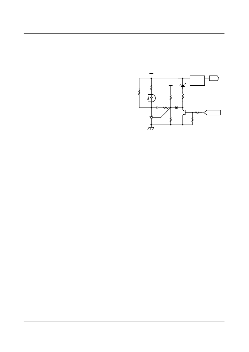
6. Burst operation :
In order to minimize the power
consumption in the standby mode, FSCQ0765RT employs
burst operation. Once FSCQ0765RT enters into burt mode,
FSCQ0765RT allows all output voltages and effective
switching frequency to be reduced. Figure 15 shows the
typical feedback circuit for C-TV applications. In normal
operation, the picture on signal is applied and the transistor
Q
1
is turned on, which de-couples R
3
, D
z
and D1 from the
feedback network. Therefore, only V
o1
is regulated by the
feedback circuit in normal operation and determined by R
1
and R
2
as
In standby mode, the picture on signal is disabled and the
transistor Q
1
is turned off, which couples R
3
, Dz and D
1
to
the reference pin of KA431. Then, Vo2 is determined by the
zener diode breakdown voltage. Assuming that the forward
voltage drop of D
1
is 0.7V, V
o2
in standby mode is approxi-
mately given by
Figure 15. Typical feedback circuit to drop output voltage
in standby mode
Figure 16 shows the burst mode operation waveforms. When
the picture ON signal is disabled, Q
1
is turned off and R
3
and Dz are connected to the reference pin of KA431 through
D
1
. Before V
o2
drops to V
o2
stby
, the voltage on the reference
pin of KA431 is higher than 2.5V, which increases the
current through the opto LED. This pulls down the feedback
voltage (V
FB
) of FSCQ0765RT and forces FSCQ0765RT to
stop switching. If the switching is disabled longer than
1.4ms, FSCQ0765RT enters into burst operation and the
operating current is reduced from 4mA (I
OP
) to 0.35mA
(I
OB
). Since there is no switching, V
o2
decrease until it
reaches V
o2
stby
. As V
o2
reaches V
o2
stby
, the current through
the opto LED decreases allowing the feedback voltage to
rise. When the feedback voltage reaches 0.4V, FSCQ0765RT
resumes switching with a predetermined peak drain current
of 0.9A. After burst switching for 1.4ms, FSCQ0765RT
stops switching and checks the feedback voltage. If the
feedback voltage is below 0.4V, FSCQ0765RT stops
switching until the feedback voltage increases to 0.4V. If the
feedback voltage is above 0.4V, FSCQ0765RT goes back to
the normal operation.
V
o1
norm
2.5
R
--------------------
R
2
+
R
2
=
V
o2
stby
V
Z
0.7
2.5
+
+
=
Picture ON
Micom
Linear
Regulator
V
O2
V
O1
(B+)
KA431
R
2
R
1
R
3
R
bias
R
D
R
F
C
F
D
1
Q1
A
C
R
Dz
相關(guān)PDF資料 |
PDF描述 |
|---|---|
| FSCQ1565RPVDTU | Green Mode Fairchild Power Switch (FPS⑩) |
| FSD1000 | Combo Fairchild Power Switch (FPS) |
| FSD200B | Green Mode Fairchild Power Switch (FPS) |
| FSD200BM | Green Mode Fairchild Power Switch (FPS) |
| FSD210B | Green Mode Fairchild Power Switch (FPS) |
相關(guān)代理商/技術(shù)參數(shù) |
參數(shù)描述 |
|---|---|
| FSCQ1465RT | 制造商:FAIRCHILD 制造商全稱:Fairchild Semiconductor 功能描述:Green Mode Fairchild Power Switch (FPS⑩) |
| FSCQ1465RTYDTU | 功能描述:電源開關(guān) IC - 配電 POWER_CONVERSION RoHS:否 制造商:Exar 輸出端數(shù)量:1 開啟電阻(最大值):85 mOhms 開啟時(shí)間(最大值):400 us 關(guān)閉時(shí)間(最大值):20 us 工作電源電壓:3.2 V to 6.5 V 電源電流(最大值): 最大工作溫度:+ 85 C 安裝風(fēng)格:SMD/SMT 封裝 / 箱體:SOT-23-5 |
| FSCQ1565RP | 制造商:FAIRCHILD 制造商全稱:Fairchild Semiconductor 功能描述:Green Mode Fairchild Power Switch (FPS TM) |
| FSCQ1565RPSYDTU | 功能描述:電源開關(guān) IC - 配電 15A/650V QRC Power Switch RoHS:否 制造商:Exar 輸出端數(shù)量:1 開啟電阻(最大值):85 mOhms 開啟時(shí)間(最大值):400 us 關(guān)閉時(shí)間(最大值):20 us 工作電源電壓:3.2 V to 6.5 V 電源電流(最大值): 最大工作溫度:+ 85 C 安裝風(fēng)格:SMD/SMT 封裝 / 箱體:SOT-23-5 |
| FSCQ1565RPVDTU | 功能描述:電源開關(guān) IC - 配電 15A/650V QRC Pwr Sw RoHS:否 制造商:Exar 輸出端數(shù)量:1 開啟電阻(最大值):85 mOhms 開啟時(shí)間(最大值):400 us 關(guān)閉時(shí)間(最大值):20 us 工作電源電壓:3.2 V to 6.5 V 電源電流(最大值): 最大工作溫度:+ 85 C 安裝風(fēng)格:SMD/SMT 封裝 / 箱體:SOT-23-5 |
發(fā)布緊急采購,3分鐘左右您將得到回復(fù)。