- 您現(xiàn)在的位置:買賣IC網(wǎng) > PDF目錄382968 > FS6261-01 (Electronic Theatre Controls, Inc.) Motherboard Clock Generator IC PDF資料下載
參數(shù)資料
| 型號(hào): | FS6261-01 |
| 廠商: | Electronic Theatre Controls, Inc. |
| 英文描述: | Motherboard Clock Generator IC |
| 中文描述: | 主板時(shí)鐘發(fā)生器IC |
| 文件頁數(shù): | 11/17頁 |
| 文件大小: | 216K |
| 代理商: | FS6261-01 |
XT
January 2000
1.31.00
11
)6
0RWKHUERDUG&ORFN*HQHUDWRU,&
,62
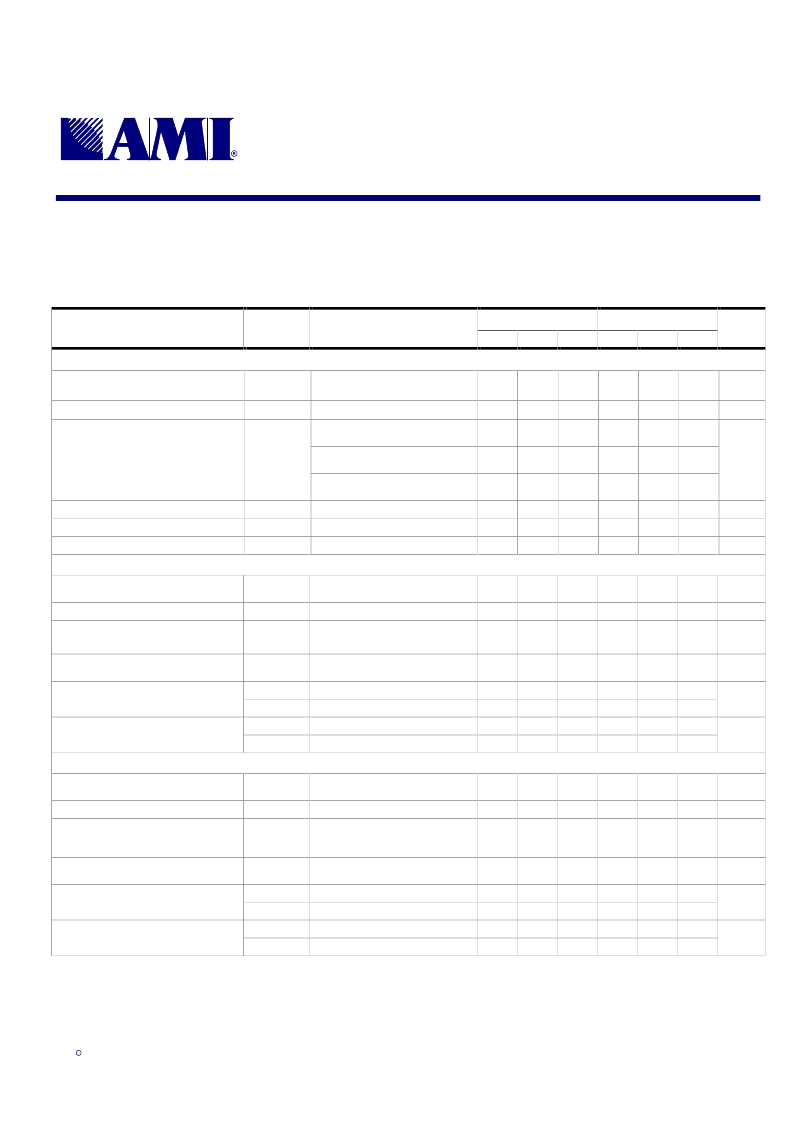
Table 9: AC Timing Specifications
Unless otherwise stated, all power supplies = 3.3V ± 10%, no load on any output, and ambient temperature range T
= 0°C to 70°C. Parameters denoted with an asterisk ( * ) represent nominal
characterization data and are not currently production tested to any specific limits. MIN and MAX characterization data are
±
3
σ
from typical. Negative currents indicate current flows out of the device.
Spread spectrum modulation is disabled except for Rise/Fall time measurements.
133MHz
100MHz
PARAMETER
SYMBOL
CONDITIONS/DESCRIPTION
MIN.
TYP.
MAX.
MIN.
TYP.
MAX.
UNITS
Overall
Spread Spectrum Modulation
Frequency *
f
m
SS_EN# low
31.5
31.5
kHz
Spread Spectrum Modulation Index*
δ
m
SS_EN# low
-0.5
-0.5
%
CPU @ 1.25V, C
=20pF to CK66 @
1.5V, C
L
=30pF (rising edges)
0
0.3
1.5
0
0.4
1.5
CK66 @ 1.5V, C
=30pF to PCI @
1.5V, C
L
=30pF (rising edges)
1.5
2.9
4.0
1.5
3.1
4.0
Clock Offset
t
pd
CPU @ 1.25V, C
=20pF to APIC @
1.25V, C
L
=20pF (rising edges)
SEL_0:1 and SEL_133/100#=0
SEL_0:1 and SEL_133/100#=0
via PWR_DWN#
1.5
2.3
4.0
1.5
3.3
4.0
ns
Tristate Enable Delay *
Tristate Disable Delay *
Clock Stabilization (on power-up) *
t
DZL,
t
DZH
t
DZL,
t
DZH
t
STB
1.0
1.0
10
10
3.0
1.0
1.0
10
10
3.0
ns
ns
ms
APIC_0:2 Clock Output (2.5V Type 1 Clock Buffer)
Duty Cycle *
d
t
Ratio of high pulse width to one
clock period, measured at 1.5V
45
50
55
45
50
55
%
Clock Skew *
t
skw
APIC to APIC @ 1.25V, C
L
=20pF
-70
-70
Jitter, Long Term (
σ
y
(
τ
)) *
t
j(LT)
On rising edges 500
μ
s apart at 1.25V
relative to an ideal clock, C
L
=20pF, all
PLLs active
204
122
ps
Jitter, Period (peak-peak) *
t
j(
P)
From rising edge to rising edge at
1.25V, C
L
=20pF, all PLLs active
82
88
ps
t
r min
t
r max
t
f min
t
f max
Measured @ 0.4V – 2.0V; C
L
=10pF
1.2
1.5
1.8
2.1
1.2
1.5
1.5
1.8
Rise Time *
Measured @ 0.4V – 2.0V; C
L
=20pF
ns
Measured @ 2.0V – 0.4V; C
L
=10pF
Fall Time *
Measured @ 2.0V – 0.4V; C
L
=20pF
ns
CPU/2_0:1 Clock Outputs (2.5V Type 1 Clock Buffer)
Duty Cycle *
d
t
Ratio of high pulse width to one
clock period, measured at 1.5V
45
52
55
45
52
55
%
Clock Skew *
t
skw
CPU/2 to CPU/2 @ 1.25V, C
L
=20pF
+10
+10
Jitter, Long Term (
σ
y
(
τ
)) *
t
j(LT)
On rising edges 500
μ
s apart at
1.25V relative to an ideal clock,
C
L
=20pF, all PLLs active
136
122
ps
Jitter, Period (peak-peak) *
t
j(
P)
From rising edge to rising edge at
1.25V, C
L
=20pF, all PLLs active
108
112
ps
t
r min
t
r max
t
f min
t
f max
Measured @ 0.4V – 2.0V; C
L
=10pF
0.9
1.1
1.0
1.2
0.8
1.1
1.0
1.2
Rise Time *
Measured @ 0.4V – 2.0V; C
L
=20pF
ns
Measured @ 2.0V – 0.4V; C
L
=10pF
Fall Time *
Measured @ 2.0V – 0.4V; C
L
=20pF
ns
相關(guān)PDF資料 |
PDF描述 |
|---|---|
| FS6284 | Dual PLL Clock Generator IC |
| FS6284-01 | Dual PLL Clock Generator IC |
| FS6322-05 | Three-PLL Clock Generator IC |
| FS6322-08 | THREE PLL CLOCK GENERATOR IC |
| FS6330 | LAN HUB CLOCK GENERATOR IC |
相關(guān)代理商/技術(shù)參數(shù) |
參數(shù)描述 |
|---|---|
| FS6282 | 制造商:未知廠家 制造商全稱:未知廠家 功能描述:DUAL PLL CLOCK GENERATOR IC |
| FS6282-03 | 制造商:未知廠家 制造商全稱:未知廠家 功能描述:DUAL PLL CLOCK GENERATOR IC |
| FS6284 | 制造商:未知廠家 制造商全稱:未知廠家 功能描述:Dual PLL Clock Generator IC |
| FS6284-01 | 制造商:未知廠家 制造商全稱:未知廠家 功能描述:Dual PLL Clock Generator IC |
| FS6322-04 | 制造商:未知廠家 制造商全稱:未知廠家 功能描述:Three-PLL Clock Generator IC |
發(fā)布緊急采購,3分鐘左右您將得到回復(fù)。