- 您現(xiàn)在的位置:買賣IC網(wǎng) > PDF目錄382968 > FS6261-01 (Electronic Theatre Controls, Inc.) Motherboard Clock Generator IC PDF資料下載
參數(shù)資料
| 型號(hào): | FS6261-01 |
| 廠商: | Electronic Theatre Controls, Inc. |
| 英文描述: | Motherboard Clock Generator IC |
| 中文描述: | 主板時(shí)鐘發(fā)生器IC |
| 文件頁(yè)數(shù): | 1/17頁(yè) |
| 文件大?。?/td> | 216K |
| 代理商: | FS6261-01 |
當(dāng)前第1頁(yè)第2頁(yè)第3頁(yè)第4頁(yè)第5頁(yè)第6頁(yè)第7頁(yè)第8頁(yè)第9頁(yè)第10頁(yè)第11頁(yè)第12頁(yè)第13頁(yè)第14頁(yè)第15頁(yè)第16頁(yè)第17頁(yè)
XT
January 2000
Intel and Pentium are registered trademarks of Intel Corporation. Spread spectrum modulation is licensed under US Patent No. 5488627, Lexmark International, Inc. American Microsystems, Inc.
reserves the right to change the detail specifications as may be required to permit improvements in the design of its products.
,62
1.31.00
)6
0RWKHUERDUG&ORFN*HQHUDWRU,&
1.0 Features
Generates clocks required for Intel
i820 based
desktop and workstation systems, including:
Four enabled 2.5V 133/100MHz CPU Front Side
Bus (FSB) clocks
Two 2.5V CPU/2 clocks for synchronous memory
Seven enabled 3.3V PCI bus clocks and one
free-running PCI clock
Four enabled 3.3V 66MHz AGP clocks
Three 2.5V 16.67MHz APIC bus clocks
Two 3.3V 14.318MHz REF clocks
One 3.3V 48MHz USB clock
CPU clock cycle – cycle jitter < 150ps p-p
Non-linear spread-spectrum modulation
(-0.5% at 31.5kHz)
Supports test mode and tristate output control
Separate CPU-enable, PCI-enable and power-down
inputs with glitch-free stop clock controls on all clocks
for clock control and power management
Figure 1: Block Diagram
Crystal
Oscillator
CK48
REF_0:1
APIC_0:2
SEL_0:1
SS_EN#
XOUT
CPU/2_0:1
PCI_1:7
VSS_P
XIN
CPU_STOP#
PCI_STOP#
PWR_DWN#
delay
FS6261-01
VDD_R
VSS_R
VDD_A
VSS_A
VSS_C
VDD_C
VDD_P
VDD_48
VSS_48
(2.5V outputs)
SEL_133/100#
PCI_F
÷6 or
÷8
CPU_0:3
VSS_C2
VDD_C2
÷3 or
÷4
VSS_66
VDD_66
CK66_0:3
delay
÷1
or ÷2
÷2
delay
PLL
PLL
÷3 or
÷4
2.0 Description
The FS6261-01 is a CMOS clock generator IC designed
for high-speed motherboard applications. Two different
frequencies can be selected for the CPU clocks via two
SEL pins. Glitch-free stop clock control of the CPU, AGP
(66MHz) and PCI clocks is provided. A low current
power-down mode is available for mobile applications.
Separate clock buffers provide for a 2.5V voltage range
on the CPU_0:3, CPU/2_0:1 and APIC_0:2 clocks.
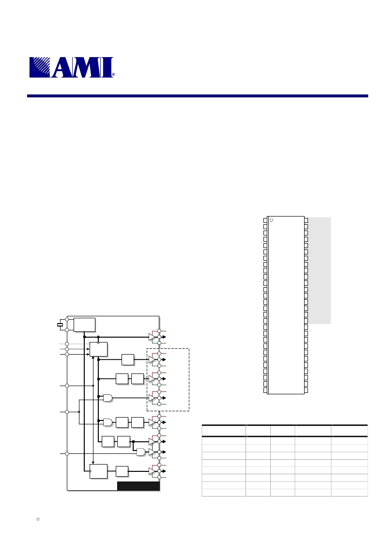
Figure 2: Pin Configuration
1
48
2
3
4
5
6
7
8
47
46
45
44
43
42
41
REF_0
REF_1
VSS_R
XIN
XOUT
VSS_P
PCI_1
CPU_2
CPU_3
VSS_A
VDD_A
APIC_0
9
10
11
12
13
14
15
16
PCI_2
VSS_P
PCI_3
PCI_4
PCI_5
PCI_6
VDD_P
PCI_7
17
18
19
20
21
22
23
VSS_P
CK66_0
CK66_1
40
39
38
37
36
35
34
33
VDD
CPU_1
CPU_0
VDD_C
VSS_C
32
31
30
29
SEL_0
SS_EN#
PCI_STOP#
CPU_STOP#
VSS
24
F
PCI_F
VDD_P
PWR_DWN#
VSS_C
VDD_C
APIC_1
(
25
26
27
28
54
53
52
51
50
49
56
55
VSS_48
VDD_48
CK48
VDD_R
VSS_66
VDD_66
VSS_66
CK66_2
CK66_3
VDD_66
SEL133/100#
SEL_1
VSS_C2
CPU/2_0
CPU/2_1
VDD_C2
APIC_2
56-pin SSOP
Table 1: CPU/PCI Frequency Selection
SEL_133/100#
SEL_1
SEL_0
CPU (MHz)
PCI (MHz)
0
0
0
0
1
1
1
1
0
0
1
1
0
0
1
1
0
1
0
1
0
1
0
1
tristate
(reserved)
100
100
XIN/2
(reserved)
133
133
tristate
(reserved)
33.33
33.33
XIN/6
(reserved)
33.33
33.33
相關(guān)PDF資料 |
PDF描述 |
|---|---|
| FS6284 | Dual PLL Clock Generator IC |
| FS6284-01 | Dual PLL Clock Generator IC |
| FS6322-05 | Three-PLL Clock Generator IC |
| FS6322-08 | THREE PLL CLOCK GENERATOR IC |
| FS6330 | LAN HUB CLOCK GENERATOR IC |
相關(guān)代理商/技術(shù)參數(shù) |
參數(shù)描述 |
|---|---|
| FS6282 | 制造商:未知廠家 制造商全稱:未知廠家 功能描述:DUAL PLL CLOCK GENERATOR IC |
| FS6282-03 | 制造商:未知廠家 制造商全稱:未知廠家 功能描述:DUAL PLL CLOCK GENERATOR IC |
| FS6284 | 制造商:未知廠家 制造商全稱:未知廠家 功能描述:Dual PLL Clock Generator IC |
| FS6284-01 | 制造商:未知廠家 制造商全稱:未知廠家 功能描述:Dual PLL Clock Generator IC |
| FS6322-04 | 制造商:未知廠家 制造商全稱:未知廠家 功能描述:Three-PLL Clock Generator IC |
發(fā)布緊急采購(gòu),3分鐘左右您將得到回復(fù)。