- 您現(xiàn)在的位置:買(mǎi)賣(mài)IC網(wǎng) > PDF目錄67592 > FS6131-01G (ON SEMICONDUCTOR) PLL FREQUENCY SYNTHESIZER, 27 MHz, PDSO16 PDF資料下載
參數(shù)資料
| 型號(hào): | FS6131-01G |
| 廠商: | ON SEMICONDUCTOR |
| 元件分類(lèi): | PLL合成/DDS/VCOs |
| 英文描述: | PLL FREQUENCY SYNTHESIZER, 27 MHz, PDSO16 |
| 封裝: | 0.150 INCH, GREEN, SOP-16 |
| 文件頁(yè)數(shù): | 24/40頁(yè) |
| 文件大小: | 746K |
| 代理商: | FS6131-01G |
第1頁(yè)第2頁(yè)第3頁(yè)第4頁(yè)第5頁(yè)第6頁(yè)第7頁(yè)第8頁(yè)第9頁(yè)第10頁(yè)第11頁(yè)第12頁(yè)第13頁(yè)第14頁(yè)第15頁(yè)第16頁(yè)第17頁(yè)第18頁(yè)第19頁(yè)第20頁(yè)第21頁(yè)第22頁(yè)第23頁(yè)當(dāng)前第24頁(yè)第25頁(yè)第26頁(yè)第27頁(yè)第28頁(yè)第29頁(yè)第30頁(yè)第31頁(yè)第32頁(yè)第33頁(yè)第34頁(yè)第35頁(yè)第36頁(yè)第37頁(yè)第38頁(yè)第39頁(yè)第40頁(yè)
30
AMI Semiconductor - Rev. 2.0, Jun. 05
www.amis.com
FS6131-01/FS6131-01g Programmable Line Lock Clock Generator IC
Data Sheet
11.1.1 Example Calculation
In PECL mode, the output driver does not source current, so the VIH value is determined by the ratios of the terminating resistors using the
equation
2
1
p
CC
NMH
R
V
+
=
where Rp1 is the pull-up resistor, Rp2 is the pull-down resistor and VNMH is the desired noise margin, and
NMH
CC
IH
V
-
=
The resistor ratio must also match the line impedance via the equation
2
1
2
1
p
L
R
z
+
=
where zL is the line impedance.
Combining these equations, and solving for Rp1 gives
÷÷
è
-
+
=
NMH
CC
NMH
L
p
V
z
R
1
If the load's VIH(min) = VCC - 0.6, choose a VNMH = 0.45V. If the line impedance is 75
W, then Rp1 is about 82W. Substituting into the equation for line
impedance and solving for Rp2 gives a value of 880
W (choose 910W).
To solve for the load's VIL, an output sink current must be programmed via the IPRG pin. If the desired VIH = VCC - 1.6, choose VCC - 2.0 for some
extra margin. A sink current of 25mA through the 82
W resistor generates a 2.05V drop. The sink current is programmed via the IPRG pin, where
the ratio of IPRG current to output sink current is 1:4. An IPRG programming resistor of 750
W at VDD = 5V generates 6.6mA, or about 27mA output
sink current.
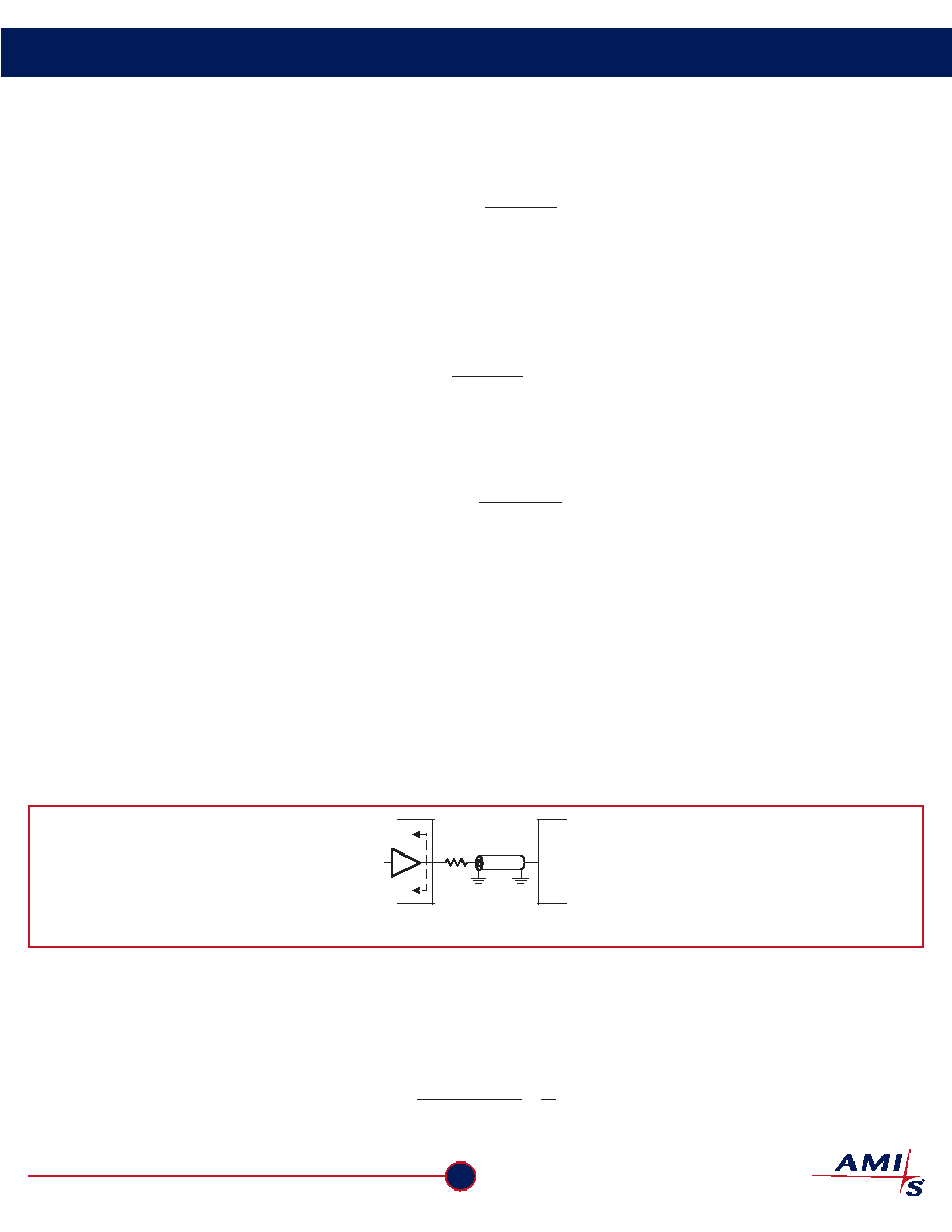
11.2 CMOS Output Mode
If a CMOS interface is desired, a transmission line is typically terminated using a series termination. Series termination adds no dc loading to the
driver, and requires less power than other resistive termination methods. In addition, no extra impedance exists from the signal line to a reference
voltage, such as ground.
R
S
z
L
z
O
DRIVER
RECEIVE
LINE
Figure 23: Series Termination (CMOS)
As shown in Figure 23, the sum of the driver's output impedance (zO) and the series termination resistance (RS) must equal the line impedance
(zL). That is,
O
L
S
z
R
-
=
When the source impedance (zO+RS) is matched to the line impedance, then by voltage division the incident wave amplitude is one-half of the full
signal amplitude.
2
)
(
)
(
V
z
R
z
R
z
V
L
S
O
S
O
i
=
+
=
相關(guān)PDF資料 |
PDF描述 |
|---|---|
| FS6131-01G | PLL FREQUENCY SYNTHESIZER, 27 MHz, PDSO16 |
| FS6131-01 | PLL FREQUENCY SYNTHESIZER, 27 MHz, PDSO16 |
| FS6131-01 | PLL FREQUENCY SYNTHESIZER, 27 MHz, PDSO16 |
| FS6S0965R-YDTU | 36 A SWITCHING REGULATOR, 150 kHz SWITCHING FREQ-MAX, PZFM5 |
| FS6S0965R-TU | 36 A SWITCHING REGULATOR, 150 kHz SWITCHING FREQ-MAX, PSFM5 |
相關(guān)代理商/技術(shù)參數(shù) |
參數(shù)描述 |
|---|---|
| FS6131-01G-XTD | 功能描述:時(shí)鐘發(fā)生器及支持產(chǎn)品 I2C PROG PLL CLK RoHS:否 制造商:Silicon Labs 類(lèi)型:Clock Generators 最大輸入頻率:14.318 MHz 最大輸出頻率:166 MHz 輸出端數(shù)量:16 占空比 - 最大:55 % 工作電源電壓:3.3 V 工作電源電流:1 mA 最大工作溫度:+ 85 C 安裝風(fēng)格:SMD/SMT 封裝 / 箱體:QFN-56 |
| FS6131-01G-XTP | 功能描述:時(shí)鐘發(fā)生器及支持產(chǎn)品 I2C PROG PLL CLK RoHS:否 制造商:Silicon Labs 類(lèi)型:Clock Generators 最大輸入頻率:14.318 MHz 最大輸出頻率:166 MHz 輸出端數(shù)量:16 占空比 - 最大:55 % 工作電源電壓:3.3 V 工作電源電流:1 mA 最大工作溫度:+ 85 C 安裝風(fēng)格:SMD/SMT 封裝 / 箱體:QFN-56 |
| FS6131-01I-XTD | 功能描述:時(shí)鐘發(fā)生器及支持產(chǎn)品 I2C PROG PLL CLK (IND) RoHS:否 制造商:Silicon Labs 類(lèi)型:Clock Generators 最大輸入頻率:14.318 MHz 最大輸出頻率:166 MHz 輸出端數(shù)量:16 占空比 - 最大:55 % 工作電源電壓:3.3 V 工作電源電流:1 mA 最大工作溫度:+ 85 C 安裝風(fēng)格:SMD/SMT 封裝 / 箱體:QFN-56 |
| FS6131-01I-XTP | 功能描述:時(shí)鐘發(fā)生器及支持產(chǎn)品 I2C PROG PLL CLK IND RoHS:否 制造商:Silicon Labs 類(lèi)型:Clock Generators 最大輸入頻率:14.318 MHz 最大輸出頻率:166 MHz 輸出端數(shù)量:16 占空比 - 最大:55 % 工作電源電壓:3.3 V 工作電源電流:1 mA 最大工作溫度:+ 85 C 安裝風(fēng)格:SMD/SMT 封裝 / 箱體:QFN-56 |
| FS6186-16/24 | 制造商:Schaffner 功能描述: |
發(fā)布緊急采購(gòu),3分鐘左右您將得到回復(fù)。