- 您現(xiàn)在的位置:買(mǎi)賣(mài)IC網(wǎng) > PDF目錄370152 > FB2033BB (NXP SEMICONDUCTORS) 8-bit latched/registered/pass-thru Futurebus universal interface transceiver PDF資料下載
參數(shù)資料
| 型號(hào): | FB2033BB |
| 廠商: | NXP SEMICONDUCTORS |
| 元件分類(lèi): | 通用總線功能 |
| 英文描述: | 8-bit latched/registered/pass-thru Futurebus universal interface transceiver |
| 中文描述: | TTL/H/L SERIES, 8-BIT REGISTERED TRANSCEIVER, INVERTED OUTPUT, PQFP52 |
| 封裝: | PLASTIC, QFP-52 |
| 文件頁(yè)數(shù): | 6/10頁(yè) |
| 文件大?。?/td> | 173K |
| 代理商: | FB2033BB |

Philips Semiconductors
Product specification
FB2033
8-bit latched/registered/pass-thru
Futurebus+ universal interface transceiver
1995 May 25
6
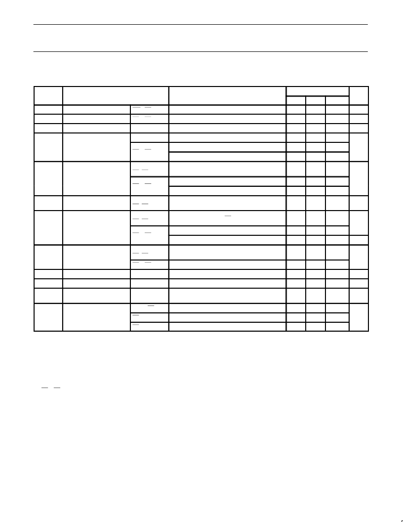
DC ELECTRICAL CHARACTERISTICS
Over recommended operating free-air temperature range unless otherwise noted.
SYMBOL
PARAMETER
TEST CONDITIONS
1
LIMITS
TYP
2
UNIT
MIN
MAX
I
OH
I
OFF
V
OH
High level output current
B0 – Bn
V
CC
= MAX, V
IL
= MAX, V
IH
= MIN, V
OH
= 1.9V
V
CC
= 0.0V, V
IL
= MAX, V
IH
= MIN, V
OH
= 1.9V
V
CC
= MIN, V
IL
= MAX, V
IH
= MIN, I
OH
= -3mA
V
CC
= MIN, V
IL
= MAX, V
IH
= MIN, I
OL
= 24mA
V
CC
= MIN, V
IL
= MAX, V
IH
= MIN, I
OL
= 100mA
V
CC
= MIN, V
IL
= MAX, V
IH
= MIN, I
OL
= 4mA
100
μ
A
μ
A
Power-off output current
B0 – Bn
AO0 – AOn
4
AO0 – AOn
4
100
High-level output voltage
2.5
2.85
V
V
OL
Low-level output voltage
0.5
V
B0 – Bn
.75
1.0
1.15
0.5
V
IK
Input clamp voltage
Except
B0–Bn
V
CC
= MIN, I
I
= I
IK
-0.5
V
B0 – Bn
V
CC
= MIN, I
I
= I
IK 6
V
CC
= MIN, I
I
= -18mA
0.3
-1.2
I
I
Input current at maximum
input voltage
Except
B0–Bn
V
CC
= MAX, V
I
= 0.0V or 5.5V
±
50
μ
A
I
IH
High-level input current
Except
B0–Bn
V
CC
= MAX, V
I
= 2.7V, Bn = AIn = 0V
20
μ
A
B0 – Bn
V
CC
= MAX, V
I
= 1.9V
V
CC
= MAX, V
I
= 3.5V
5
100
100
mA
I
IL
Low-level input current
Except
B0–Bn
V
CC
= MAX, V
I
= 0.5V
-20
μ
A
B0 – Bn
V
CC
= MAX, V
I
= 0.75V
V
CC
= MAX, V
O
= 2.7V
V
CC
= MAX, V
O
= 0.5V
-100
I
OZH
I
OZL
Off-state output current
AO0 – AOn
50
μ
A
μ
A
Off-state output current
AO0 – AOn
-50
I
OS
Short-circuit output
current
3
AO0 – AOn
only
V
CC
= MAX, V
O
= 0.0V
-45
-150
mA
I
CC
Supply current (total)
AIn to Bn
V
CC
= MAX, outputs Low or High
V
CC
= MAX, outputs Low
V
CC
= MAX, outputs High
24
50
mA
Bn to AOn
45
75
Bn to AOn
22
44
NOTES:
1. For conditions shown as MIN or MAX, use the appropriate value specified under recommended operation conditions for the applicable type.
2. All typical values are at V
= 5V, T
= 25
°
C.
3. Not more than one output should be shorted at a time. For testing I
OS
, the use of high-speed test apparatus and/or sample-and-hold
techniques are preferable in order to minimize internal heating and more accurately reflect operational values. Otherwise, prolonged shorting
of a High output may raise the chip temperature well above normal and thereby cause invalid readings in other parameter tests. In any
sequence of parameter tests, I
OS
tests should be performed last.
4. Due to test equipment limitations, actual test conditions are V
IH
= 1.8V and V
IL
= 1.3V for the B side.
5. For B port input voltage between 3 and 5 volts I
IH
will be greater than 100
μ
A, but the parts will continue to function normally.
6. B0 – B7 clamps remain active for a minimum of 80ns following a High-to-Low transition.
相關(guān)PDF資料 |
PDF描述 |
|---|---|
| FB2040A | 8-bit Futurebus transceiver |
| FB2040BB | 8-bit Futurebus transceiver |
| FB2041BB-T | 7-Bit Bus Transceiver |
| FB2041 | 7-bit Futurebus+ transceiver(7位預(yù)置總線收發(fā)器) |
| FB2041BB | 7-bit Futurebus transceiver |
相關(guān)代理商/技術(shù)參數(shù) |
參數(shù)描述 |
|---|---|
| FB2033BB-T | 制造商:未知廠家 制造商全稱(chēng):未知廠家 功能描述:Single 8-Bit Inverting Bus Transceiver |
| FB2033K | 制造商:TI 制造商全稱(chēng):Texas Instruments 功能描述:8-BIT TTL/BTL REGISTERED TRANSCEIVER |
| FB-20-4 | 制造商:Polycase 功能描述:Enclosure |
| FB2040 | 制造商:TI 制造商全稱(chēng):Texas Instruments 功能描述:8-BIT TTL/BTL TRANSCEIVER |
| FB20401 | 制造商:Marathon Special Products 功能描述: |
發(fā)布緊急采購(gòu),3分鐘左右您將得到回復(fù)。