- 您現(xiàn)在的位置:買賣IC網(wǎng) > PDF目錄67412 > FA7738P (FUJI ELECTRIC CO LTD) 5.5 A SWITCHING REGULATOR, 400 kHz SWITCHING FREQ-MAX, PDIP8 PDF資料下載
參數(shù)資料
| 型號(hào): | FA7738P |
| 廠商: | FUJI ELECTRIC CO LTD |
| 元件分類: | 穩(wěn)壓器 |
| 英文描述: | 5.5 A SWITCHING REGULATOR, 400 kHz SWITCHING FREQ-MAX, PDIP8 |
| 封裝: | DIP-8 |
| 文件頁(yè)數(shù): | 4/19頁(yè) |
| 文件大小: | 484K |
| 代理商: | FA7738P |
第1頁(yè)第2頁(yè)第3頁(yè)當(dāng)前第4頁(yè)第5頁(yè)第6頁(yè)第7頁(yè)第8頁(yè)第9頁(yè)第10頁(yè)第11頁(yè)第12頁(yè)第13頁(yè)第14頁(yè)第15頁(yè)第16頁(yè)第17頁(yè)第18頁(yè)第19頁(yè)

12
FA7738N/P
8. Operation description of each block
(1) Reference voltage circuit
The reference voltage circuit generates an output
return voltage (VIN) of 1.00 V ± 1% for which
temperature compensation is provided by the VCC
voltage, along with an internal control power
(VREG) of 3.0 V.
The output return voltage (VIN) is connected to the
non-reverse input of the error amplifier (OTA) and
constitutes the reference voltage of the error
amplifier.
The power VREG voltage supply of the internal
control system is output from the CREG terminal
and is connected with the capacitor CREG for
stabilization.
This voltage is designed specifically for the control
power of all IC internal circuits. It therefore cannot
be used as an external stabilization power supply.
To connect the CREG capacity of the stabilization
capacitor
to
the
CREG
terminal,
see
the
recommended operating conditions.
(2) Oscillator
This oscillator is based on capacitor charge and
discharge.
Its oscillation frequency
can be set to a desired level based on
the RT of the resistor to be connected
to the RT terminal (Fig. 1).
(A high RT means a low operating
frequency.
A low RT means a high operating
frequency.)
Set the oscillation frequency to any
setting between 30 kHz and 400 kHz.
The RT terminal outputs DC voltage of about 1 V.
(3) Error amplifier (OTA)
The IN terminal (No. 5) is a reverse input terminal.
The non-reverse input is connected to a reference
voltage (VIN) with 1.0 V ± 1% inside the IC. The FB
terminal is not exposed outside and performs phase
compensation inside the IC.
Voltage is supplied to the IN terminal as a
resistance-divided voltage from the output voltage of
the DC-DC converter circuit. The output voltage
Vout of the DC-DC converter can be determined by:
IN
V
R
Vout
×
+
=
2
1
Note that, if the unit
does
not
operate
stably depending on
the input conditions,
capacitor C1 can be
connected to it for
phase
adjustment
and enhancement.
(4) PWM comparator
The ON state of output (from the OUT terminal)
starts with the ON signal of the oscillator.
It is
turned off when the coil current reaches the level
specified by the output (OTA output) of the error
amplifier.
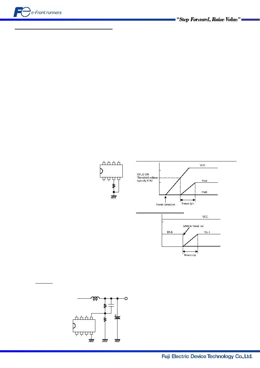
(5) Soft starter
This unit incorporates a soft starter to prevent the
DC-DC converter circuit from anomalous operation
(such as a rush current) at startup.
A soft start is made by gradually increasing the
output by progressively raising the reference voltage
of the error amplifier (OTA).
The soft start time is fixed at 8 msec (typically)
inside the IC.
This refers to the time from when power is turned on
to when the input voltage reaches the ON threshold
voltage (typically 6.9 V) or more of the low-voltage
malfunction prevention circuit (Fig. 3).
Once power is supplied, an ENB signal initiates a
soft start.
Power supply startup from when the ENB signal is set to low state
Startup by an ENB signal
Fig. 3
12
3
4
87
6
5
CREG
ENB
RT
GND
VCC
OUT
VBIAS
IN
RT
Fig.1
12
34
87
65
CREG
ENB
RT
GND
VCC
OUT
VBIAS
IN
Vout
R1
R2
C1
Fig.2
相關(guān)PDF資料 |
PDF描述 |
|---|---|
| FAB2200UCX | 1.2 W, 2 CHANNEL, AUDIO AMPLIFIER, PBGA25 |
| FAN3850AUC19X | SPECIALTY CONSUMER CIRCUIT, PBGA6 |
| FAN4040DIS3-3.3 | 1-OUTPUT TWO TERM VOLTAGE REFERENCE, 3.3 V, PDSO3 |
| FAN4040CIS3-2.5 | 1-OUTPUT TWO TERM VOLTAGE REFERENCE, 2.5 V, PDSO3 |
| FAN4040AIS3-3.3 | 1-OUTPUT TWO TERM VOLTAGE REFERENCE, 3.3 V, PDSO3 |
相關(guān)代理商/技術(shù)參數(shù) |
參數(shù)描述 |
|---|---|
| FA7764 | 制造商:FUJI 制造商全稱:Fuji Electric 功能描述:FUJI Power Supply Control IC |
| FA77B3 031660 | 制造商:Comair Rotron 功能描述:FAN 172MM 240VAC |
| FA77B3 31660 | 制造商:Comair Rotron 功能描述:FAN 171MM 240VAC |
| FA780 | 制造商:Black Box Corporation 功能描述:DB9/RJ12 MALE MODULAR ADAPTER, RED |
| FA781 | 制造商:Black Box Corporation 功能描述:DB9 Colored Modular Adapter (Unassembled), Male to RJ-11, 6-Wire, Green |
發(fā)布緊急采購(gòu),3分鐘左右您將得到回復(fù)。