- 您現(xiàn)在的位置:買賣IC網(wǎng) > PDF目錄362800 > EVAL-AD1992EB (Analog Devices, Inc.) Audio Switching Amplifier PDF資料下載
參數(shù)資料
| 型號: | EVAL-AD1992EB |
| 廠商: | Analog Devices, Inc. |
| 英文描述: | Audio Switching Amplifier |
| 中文描述: | 音頻開關(guān)放大器 |
| 文件頁數(shù): | 14/20頁 |
| 文件大?。?/td> | 346K |
| 代理商: | EVAL-AD1992EB |
AD1992
Note that the amplifier is capable of dc-coupled operation if the
circuit includes some means to account for this bias voltage.
Rev. 0 | Page 14 of 20
AINL/
AINR
0V
+
0
Figure 34. AC-Coupled Input Signal
Setting the Modulator Gain
The AD1992 modulator uses a combination of the input signal
and feedback from the power output stage to calculate its two-
state output pattern. The feedback input nodes are part of the
internal analog circuit that operates from the AV
DD
(nominal
5 V) power supply. Because the voltage measured at the power
outputs is nominally between 0 V and PV
DD
, and thus beyond
the 0 V to AV
DD
range, a voltage divider is required to scale the
feedback to an appropriate level.
Resistor voltage dividers should sense the voltage on each side
of the differential output and provide these feedback signals to
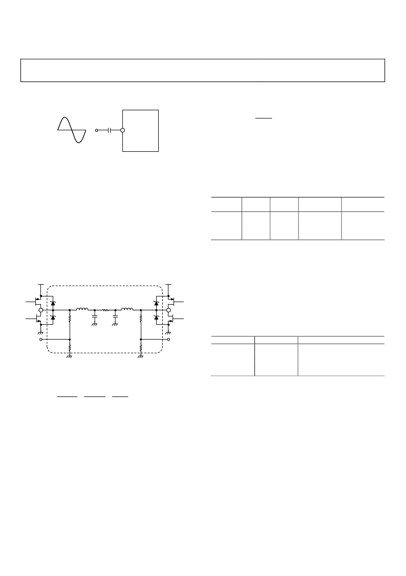
the modulator, as shown in Figure 35.
EXTERNAL COMPONENTS
R1
R3
C
C
L
L
R
L
D2
D4
D1
D3
OUTx+
OUTx–
R2
R4
PV
DD
PV
DD
NFx+
NFx–
PGND
PGND
0
Figure 35. H-Bridge Configuration
The resistor values should satisfy the following equation to
maintain modulator stability.
3
2
R
R
635
.
4
4
2
1
DD
PV
R
R
R
R
Gain
=
+
=
+
=
Selecting a gain that meets this criterion ensures that the
modulator remains in a stable operating condition.
The ratio of the resistances sets the gain rather than the absolute
values. However, the dividers provide a path from the high
voltage supply to ground; therefore, the values should be large
enough to produce negligible loss due to quiescent current.
The chip contains a calibration circuit to minimize voltage
offsets at the speaker, which helps to minimize clicks and pops
when muting or unmuting. Optimal performance is achieved
for the offset calibration circuit when the feedback divider resistors
sum to 6 kΩ, that is, (R1 + R2) = 6 kΩ, and (R3 + R4) = 6 kΩ.
This fixed total resistance to ground eliminates the last free
variable and gives the following equations for the resistors:
21810
=
=
DD
PV
R4
R2
R1
=
R3
= 6000
R2
Note that the gain previously mentioned applies to each side of
the differential output pair. Therefore, the total forward gain for
the modulator and output stage is twice that value. Recommended
resistor values for some common supply voltages are shown
in Table 10.
Table 10. Recommended Feedback Resistor Values
PV
DD
(V)
12
15
18
20
R1 (kΩ)
4.18
4.55
4.79
4.91
R2 (kΩ)
1.82
1.45
1.21
1.09
Voltage
Divider Gain
3.30
4.13
4.95
5.50
Differential
System Gain
6.60 (16.4 dB)
8.25 (18.3 dB)
9.90 (19.9 dB)
11.0 (20.8 dB)
Programmable Gain Amplifier (PGA)
The Σ-Δ modulator itself requires a fixed gain for a given value
of PV
DD
to maintain optimal stability. This gain can be appropriate,
but many applications require more gain to account for low
source signal levels. The AD1992 includes a programmable gain
amplifier (PGA) to boost the overall amplifier gain. The total gain
for the amplifier is the product of the modulator gain and the
PGA gain. PGA1 (Pin 31) and PGA0 (Pin 32) select one of four
PGA gain values, as shown in Table 11.
Table 11. PGA Gain Settings
PGA1
PGA0
0
0
0
1
1
0
1
1
The AD1992 incorporates a single-ended-to-differential
converter for each channel in the analog front-end section.
The PGA is also part of this analog front-end, and it affects the
analog input signal before it enters the Σ-Δ modulator. The
PGA1 and PGA0 pins are continuously monitored and allow
the gain to be changed at any time.
PGA Gain
1 (0 dB)
2 (6 dB)
4 (12 dB)
8 (18 dB)
POWER STAGE
The H-Bridge
The output stage of the AD1992 includes four integrated
MOSFET devices arranged in a full H-bridge, as shown in
Figure 35. The P-Type, high-side transistor of one leg and the
N-Type, low-side transistor of the opposite leg switch on and off
as a pair producing a total voltage swing across the load of
PV
DD
to +PV
DD
. The drive is floating and differential, and it is
important that neither output terminal be shorted to ground.
相關(guān)PDF資料 |
PDF描述 |
|---|---|
| EVAL-AD1994EB | Audio Switching Amplifier |
| EVAL-AD421EB | Loop-Powered 4 mA to 20 mA DAC |
| Eval-AD5025EBZ | Fully Accurate 12-/14-/16-Bit VOUT DAC SPI Interface 2.7 V to 5.5 V in a TSSOP |
| Eval-AD5045EBZ | Fully Accurate 12-/14-/16-Bit VOUT DAC SPI Interface 2.7 V to 5.5 V in a TSSOP |
| Eval-AD5065EBZ | Fully Accurate 12-/14-/16-Bit VOUT DAC SPI Interface 2.7 V to 5.5 V in a TSSOP |
相關(guān)代理商/技術(shù)參數(shù) |
參數(shù)描述 |
|---|---|
| EVAL-AD1994EB | 制造商:Analog Devices 功能描述:EVAL BOARD FOR AD1994 - Bulk |
| EVAL-AD1994EBZ | 制造商:Analog Devices 功能描述:EVAL BD CLASS D AUDIO POWER OUTPUT STAGE - Bulk |
| EVAL-AD22305 | 制造商:Analog Devices 功能描述:AD22305EVAL - Bulk |
| EVAL-AD22305X | 制造商:Analog Devices 功能描述:AD22305EVAL (X GRADE) - Bulk |
| EVAL-AD2S1200CB | 制造商:Analog Devices 功能描述:EVALUATION BOARD I.C. - Bulk |
發(fā)布緊急采購,3分鐘左右您將得到回復(fù)。