- 您現(xiàn)在的位置:買賣IC網(wǎng) > PDF目錄17026 > EVAL-AD1974AZ (Analog Devices Inc)BOARD EVAL FOR AD1974 PDF資料下載
參數(shù)資料
| 型號: | EVAL-AD1974AZ |
| 廠商: | Analog Devices Inc |
| 文件頁數(shù): | 1/24頁 |
| 文件大小: | 0K |
| 描述: | BOARD EVAL FOR AD1974 |
| 標準包裝: | 1 |
| ADC 的數(shù)量: | 4 |
| 位數(shù): | 24 |
| 采樣率(每秒): | 192k |
| 數(shù)據(jù)接口: | 串行 |
| 輸入范圍: | 1.9 Vrms |
| 工作溫度: | -40°C ~ 125°C |
| 已用 IC / 零件: | AD1974 |
| 已供物品: | 板 |
4 ADC with PLL,
192 kHz, 24-Bit ADC
Data Sheet
Rev. D
Information furnished by Analog Devices is believed to be accurate and reliable. However, no
responsibilityisassumedbyAnalogDevicesforitsuse,norforanyinfringementsofpatentsorother
rightsofthirdpartiesthatmayresultfromitsuse.Specificationssubjecttochangewithoutnotice.No
license is granted by implication or otherwise under any patent or patent rights of Analog Devices.
Trademarksandregisteredtrademarksarethepropertyoftheirrespectiveowners.
One Technology Way, P.O. Box 9106, Norwood, MA 02062-9106, U.S.A.
Tel: 781.329.4700
2007–2013 Analog Devices, Inc. All rights reserved.
FEATURES
Phase-locked loop generated or direct master clock
Low EMI design
107 dB dynamic range and SNR
94 dB THD + N
Single 3.3 V supply
Tolerance for 5 V logic inputs
Supports 24 bits and 8 kHz to 192 kHz sample rates
Differential ADC input
SPI-controllable for flexibility
Software-controllable clickless mute
Software power-down
Right justified, left justified, I2S, and TDM modes
Master and slave modes up to 16-channel input/output
Available in a 48-lead LQFP
Qualified for automotive applications
APPLICATIONS
Automotive audio systems
Home Theater Systems
Set-top boxes
Digital audio effects processors
GENERAL DESCRIPTION
The AD1974 is a high performance, single-chip ADC that pro-
vides four analog-to-digital converters (ADCs) with differential
inputs using the Analog Devices, Inc. patented multibit sigma-
delta (Σ-Δ) architecture. An SPI port is included, allowing a
microcontroller to enable mutes and adjust many other
parameters. The AD1974 operates from 3.3 V digital and analog
supplies. The AD1974 is available in a single-ended output
48-lead LQFP.
The AD1974 is designed for low EMI. This consideration is
apparent in both the system and circuit design architectures.
By using the on-board phase-locked loop (PLL) to derive the
master clock from the LR clock or from an external crystal,
the AD1974 eliminates the need for a separate high frequency
master clock and can also be used with a suppressed bit clock.
The ADCs are designed using the latest continuous time archi-
tectures from Analog Devices to further minimize EMI. By
using 3.3 V supplies, power consumption is minimized, further
reducing emissions.
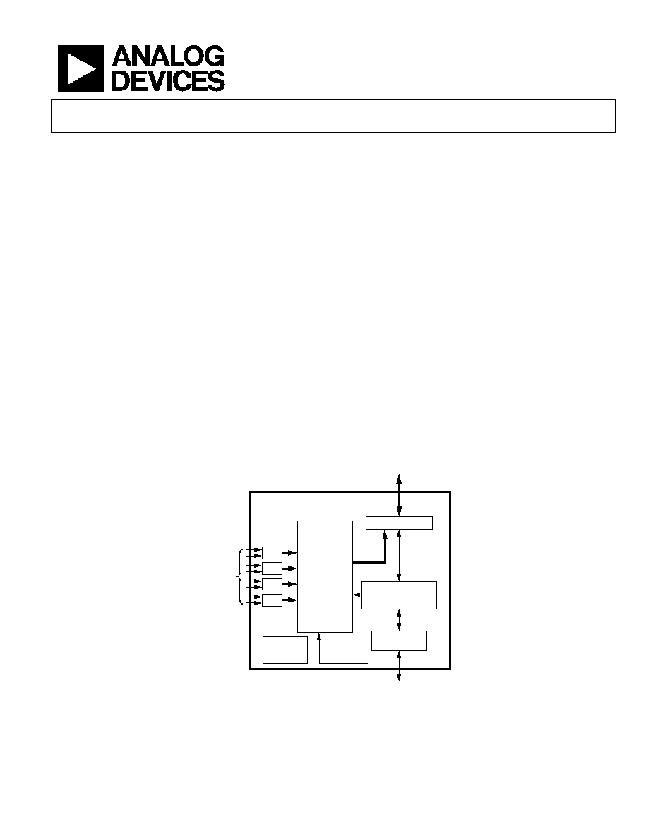
FUNCTIONAL BLOCK DIAGRAM
QUAD
DEC
FILTER
48kHz/
96kHz/192kHz
SERIAL DATA PORT
DIGITAL AUDIO
INPUT/OUTPUT
PRECISION
VOLTAGE
REFERENCE
12.48MHz
TIMING MANAGEMENT
AND CONTROL
(CLOCK AND PLL)
CONTROL PORT
SPI
CONTROL DATA
INPUT/OUTPUT
AD1974
ADC
ANALOG
AUDIO
INPUTS
SDATA
OUT
CLOCKS
06614-
001
Figure 1.
相關PDF資料 |
PDF描述 |
|---|---|
| FPF2100 | IC LOAD SWITCH FULL FUNC SOT23-5 |
| 0210391056 | CABLE JUMPER 1MM .076M 35POS |
| AD9287-100EBZ | BOARD EVALUATION AD9287 |
| VE-JWX-EY | CONVERTER MOD DC/DC 5.2V 50W |
| EVAL-AD1871EBZ | BOARD EVAL FOR AD1871 |
相關代理商/技術參數(shù) |
參數(shù)描述 |
|---|---|
| EVAL-AD1974EB | 制造商:AD 制造商全稱:Analog Devices 功能描述:4 ADC with PLL, 192 kHz, 24-Bit Codec |
| EVAL-AD1974EBZ | 制造商:Analog Devices 功能描述:EVAL KIT FOR 4 ADC W/ PLL, 192 KHZ, 24BIT CODEC EVAL-AD1974E - Boxed Product (Development Kits) |
| EVAL-AD1990EB | 制造商:Analog Devices 功能描述:EVAL BD CLASS D AUDIO POWER OUTPUT STAGE - Bulk |
| EVAL-AD1992EB | 制造商:AD 制造商全稱:Analog Devices 功能描述:Audio Switching Amplifier |
| EVAL-AD1994EB | 制造商:Analog Devices 功能描述:EVAL BOARD FOR AD1994 - Bulk |
發(fā)布緊急采購,3分鐘左右您將得到回復。