- 您現(xiàn)在的位置:買賣IC網(wǎng) > PDF目錄362753 > EPM7256B (Altera Corporation) Programmable Logic Device Family(MAX7000B可編程邏輯系列器件) PDF資料下載
參數(shù)資料
| 型號: | EPM7256B |
| 廠商: | Altera Corporation |
| 英文描述: | Programmable Logic Device Family(MAX7000B可編程邏輯系列器件) |
| 中文描述: | 可編程邏輯器件系列(MAX7000B可編程邏輯系列器件) |
| 文件頁數(shù): | 23/125頁 |
| 文件大小: | 1053K |
| 代理商: | EPM7256B |
第1頁第2頁第3頁第4頁第5頁第6頁第7頁第8頁第9頁第10頁第11頁第12頁第13頁第14頁第15頁第16頁第17頁第18頁第19頁第20頁第21頁第22頁當(dāng)前第23頁第24頁第25頁第26頁第27頁第28頁第29頁第30頁第31頁第32頁第33頁第34頁第35頁第36頁第37頁第38頁第39頁第40頁第41頁第42頁第43頁第44頁第45頁第46頁第47頁第48頁第49頁第50頁第51頁第52頁第53頁第54頁第55頁第56頁第57頁第58頁第59頁第60頁第61頁第62頁第63頁第64頁第65頁第66頁第67頁第68頁第69頁第70頁第71頁第72頁第73頁第74頁第75頁第76頁第77頁第78頁第79頁第80頁第81頁第82頁第83頁第84頁第85頁第86頁第87頁第88頁第89頁第90頁第91頁第92頁第93頁第94頁第95頁第96頁第97頁第98頁第99頁第100頁第101頁第102頁第103頁第104頁第105頁第106頁第107頁第108頁第109頁第110頁第111頁第112頁第113頁第114頁第115頁第116頁第117頁第118頁第119頁第120頁第121頁第122頁第123頁第124頁第125頁
Altera Corporation
23
MAX 7000B Programmable Logic Device Family Data Sheet
Preliminary Information
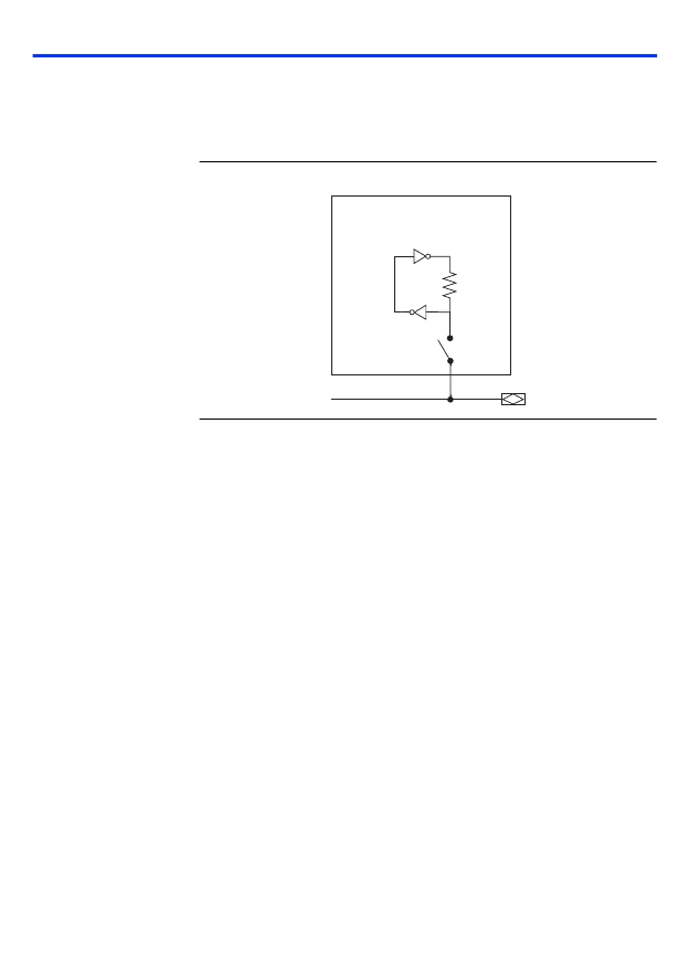
Two inverters implement the bus-hold circuitry in a loop that weakly
drives back to the I/ O pin at the end of programming.
Figure 10
shows a block diagram of the bus-hold circuit.
Figure 10. Bus-Hold Circuit
Power
Sequencing &
Hot-Socketing
Because MAX 7000B devices can be used in a mixed-voltage environment,
they have been designed specifically to tolerate any possible power-up
sequence. The V
CCIO
and V
CCINT
power planes can be powered in any
order.
Signals can be driven into MAX 7000B devices before and during power
up without damaging the device. Additionally, MAX 7000B devices do
not drive out during power up. Once operating conditions are reached,
MAX 7000B devices operate as specified by the user.
Design Security
All MAX 7000B devices contain a programmable security bit that controls
access to the data programmed into the device. When this bit is
programmed, a design implemented in the device cannot be copied or
retrieved. This feature provides a high level of design security, because
programmed data within EEPROM cells is invisible. The security bit that
controls this function, as well as all other programmed data, is reset only
when the device is reprogrammed.
Generic Testing
MAX 7000B devices are fully functionally tested. Complete testing of each
programmable EEPROM bit and all internal logic elements ensures 100
%
programming yield. AC test measurements are taken under conditions
equivalent to those shown in
Figure 11
. Test patterns can be used and then
erased during early stages of the production flow.
I/O
RBH
Bus Hold Circuit
Drive to
VCCIO level
相關(guān)PDF資料 |
PDF描述 |
|---|---|
| EPM7032LC44-15 | Programmable Logic Device Family |
| EPM7064B | Programmable Logic Device |
| EPM7128A | Programmable Logic Device |
| EPM7256A | Programmable Logic Device |
| EPM7032AE | Programmable Logic Device |
相關(guān)代理商/技術(shù)參數(shù) |
參數(shù)描述 |
|---|---|
| EPM7256BBC169-10 | 制造商:未知廠家 制造商全稱:未知廠家 功能描述:ASIC |
| EPM7256BBC169-5 | 制造商:未知廠家 制造商全稱:未知廠家 功能描述:ASIC |
| EPM7256BBC169-7 | 制造商:未知廠家 制造商全稱:未知廠家 功能描述:ASIC |
| EPM7256BBI169-10 | 制造商:未知廠家 制造商全稱:未知廠家 功能描述:ASIC |
| EPM7256BBI169-5 | 制造商:未知廠家 制造商全稱:未知廠家 功能描述:ASIC |
發(fā)布緊急采購,3分鐘左右您將得到回復(fù)。