- 您現(xiàn)在的位置:買賣IC網(wǎng) > PDF目錄11597 > ENC424J600-I/PT (Microchip Technology)IC ETHERNET CTRLR W/SPI 44-TQFP PDF資料下載
參數(shù)資料
| 型號(hào): | ENC424J600-I/PT |
| 廠商: | Microchip Technology |
| 文件頁(yè)數(shù): | 17/168頁(yè) |
| 文件大小: | 0K |
| 描述: | IC ETHERNET CTRLR W/SPI 44-TQFP |
| 視頻文件: | Fast 100 Mbps Ethernet PICtail Plus Overview |
| 標(biāo)準(zhǔn)包裝: | 160 |
| 控制器類型: | 以太網(wǎng)控制器(IEEE 802.3) |
| 接口: | SPI |
| 電源電壓: | 3 V ~ 3.6 V |
| 電流 - 電源: | 96mA |
| 工作溫度: | -40°C ~ 85°C |
| 安裝類型: | 表面貼裝 |
| 封裝/外殼: | 44-TQFP |
| 供應(yīng)商設(shè)備封裝: | 44-TQFP(10x10) |
| 包裝: | 托盤 |
| 產(chǎn)品目錄頁(yè)面: | 684 (CN2011-ZH PDF) |
| 配用: | AC164132-ND - BOARD DAUGHTER PICTAIL ETHERNET |
第1頁(yè)第2頁(yè)第3頁(yè)第4頁(yè)第5頁(yè)第6頁(yè)第7頁(yè)第8頁(yè)第9頁(yè)第10頁(yè)第11頁(yè)第12頁(yè)第13頁(yè)第14頁(yè)第15頁(yè)第16頁(yè)當(dāng)前第17頁(yè)第18頁(yè)第19頁(yè)第20頁(yè)第21頁(yè)第22頁(yè)第23頁(yè)第24頁(yè)第25頁(yè)第26頁(yè)第27頁(yè)第28頁(yè)第29頁(yè)第30頁(yè)第31頁(yè)第32頁(yè)第33頁(yè)第34頁(yè)第35頁(yè)第36頁(yè)第37頁(yè)第38頁(yè)第39頁(yè)第40頁(yè)第41頁(yè)第42頁(yè)第43頁(yè)第44頁(yè)第45頁(yè)第46頁(yè)第47頁(yè)第48頁(yè)第49頁(yè)第50頁(yè)第51頁(yè)第52頁(yè)第53頁(yè)第54頁(yè)第55頁(yè)第56頁(yè)第57頁(yè)第58頁(yè)第59頁(yè)第60頁(yè)第61頁(yè)第62頁(yè)第63頁(yè)第64頁(yè)第65頁(yè)第66頁(yè)第67頁(yè)第68頁(yè)第69頁(yè)第70頁(yè)第71頁(yè)第72頁(yè)第73頁(yè)第74頁(yè)第75頁(yè)第76頁(yè)第77頁(yè)第78頁(yè)第79頁(yè)第80頁(yè)第81頁(yè)第82頁(yè)第83頁(yè)第84頁(yè)第85頁(yè)第86頁(yè)第87頁(yè)第88頁(yè)第89頁(yè)第90頁(yè)第91頁(yè)第92頁(yè)第93頁(yè)第94頁(yè)第95頁(yè)第96頁(yè)第97頁(yè)第98頁(yè)第99頁(yè)第100頁(yè)第101頁(yè)第102頁(yè)第103頁(yè)第104頁(yè)第105頁(yè)第106頁(yè)第107頁(yè)第108頁(yè)第109頁(yè)第110頁(yè)第111頁(yè)第112頁(yè)第113頁(yè)第114頁(yè)第115頁(yè)第116頁(yè)第117頁(yè)第118頁(yè)第119頁(yè)第120頁(yè)第121頁(yè)第122頁(yè)第123頁(yè)第124頁(yè)第125頁(yè)第126頁(yè)第127頁(yè)第128頁(yè)第129頁(yè)第130頁(yè)第131頁(yè)第132頁(yè)第133頁(yè)第134頁(yè)第135頁(yè)第136頁(yè)第137頁(yè)第138頁(yè)第139頁(yè)第140頁(yè)第141頁(yè)第142頁(yè)第143頁(yè)第144頁(yè)第145頁(yè)第146頁(yè)第147頁(yè)第148頁(yè)第149頁(yè)第150頁(yè)第151頁(yè)第152頁(yè)第153頁(yè)第154頁(yè)第155頁(yè)第156頁(yè)第157頁(yè)第158頁(yè)第159頁(yè)第160頁(yè)第161頁(yè)第162頁(yè)第163頁(yè)第164頁(yè)第165頁(yè)第166頁(yè)第167頁(yè)第168頁(yè)
2007 Microchip Technology Inc.
DS39599G-page 111
PIC18F2220/2320/4220/4320
10.5
PORTE, TRISE and LATE
Registers
PORTE is available only in PIC18F4X20 devices.
PIC18F2X20 devices always will read back 0x00 from
PORTE.
For PIC18F4X20 devices, PORTE is a 4-bit wide port.
Three pins (RE0/AN5/RD, RE1/AN6/WR and RE2/
AN7/CS) are individually configurable as inputs or out-
puts. These pins have Schmitt Trigger input buffers.
When selected as an analog input, these pins will read
as ‘0’s.
The corresponding Data Direction register is TRISE.
Setting a TRISE bit (= 1) will make the corresponding
PORTE pin an input (i.e., put the corresponding output
driver in a high-impedance mode). Clearing a TRISE bit
(= 0) will make the corresponding PORTE pin an output
(i.e., put the contents of the output latch on the selected
pin).
TRISE controls the direction of the RE pins even when
they are being used as analog inputs. The user must
make sure to keep the pins configured as inputs when
using them as analog inputs.
The upper four bits of the TRISE register also control
the operation of the Parallel Slave Port. Their operation
is explained in Register 10-1.
The Data Latch register (LATE) is also memory
mapped. Read-modify-write operations on the LATE
register read and write the latched output value for
PORTE.
The fourth pin of PORTE (MCLR/VPP/RE3) is an input
only pin. Its operation is controlled by the MCLRE Con-
figuration
bit
in
Configuration
Register
3H
(CONFIG3H<7>). When selected as a port pin
(MCLRE = 0), it functions as a digital input only pin; as
such, it does not have TRIS or LAT bits associated with
its operation. Otherwise, it functions as the device’s
Master Clear input. In either configuration, RE3 also
functions as the programming voltage input during
programming.
EXAMPLE 10-5:
INITIALIZING PORTE
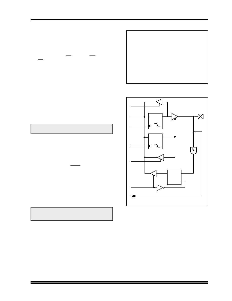
FIGURE 10-13:
BLOCK DIAGRAM OF
RE2:RE0 PINS
Note:
On a Power-on Reset, RE2:RE0 are
configured as analog inputs.
Note:
On a Power-on Reset, RE3 is enabled as
a digital input only if Master Clear
functionality is disabled.
CLRF
PORTE
; Initialize PORTE by
; clearing output
; data latches
CLRF
LATE
; Alternate method
; to clear output
; data latches
MOVLW
0x0A
; Configure A/D
MOVWF
ADCON1 ; for digital inputs
MOVLW
0x03
; Value used to
; initialize data
; direction
MOVWF
TRISC
; Set RE<0> as inputs
; RE<1> as outputs
; RE<2> as inputs
Data
Bus
WR LATE
WR TRISE
RD PORTE
Data Latch
TRIS Latch
RD TRISE
Schmitt
Trigger
Input
Buffer
Q
D
CK
Q
D
CK
EN
QD
EN
I/O pin(1)
RD LATE
or
PORTE
To Analog Converter
Note 1:
I/O pins have diode protection to VDD and VSS.
相關(guān)PDF資料 |
PDF描述 |
|---|---|
| VI-B3M-IX-F1 | CONVERTER MOD DC/DC 10V 75W |
| VI-B3M-IW-F2 | CONVERTER MOD DC/DC 10V 100W |
| VI-B3L-IX-F4 | CONVERTER MOD DC/DC 28V 75W |
| VI-B3L-IX-F2 | CONVERTER MOD DC/DC 28V 75W |
| VI-B3L-IW-F4 | CONVERTER MOD DC/DC 28V 100W |
相關(guān)代理商/技術(shù)參數(shù) |
參數(shù)描述 |
|---|---|
| ENC424J600T-I/ML | 功能描述:以太網(wǎng) IC 10/100 Base-T Stand alone Ethernet Ctrlr RoHS:否 制造商:Micrel 產(chǎn)品:Ethernet Switches 收發(fā)器數(shù)量:2 數(shù)據(jù)速率:10 Mb/s, 100 Mb/s 電源電壓-最大:1.25 V, 3.45 V 電源電壓-最小:1.15 V, 3.15 V 最大工作溫度:+ 85 C 封裝 / 箱體:QFN-64 封裝:Tray |
| ENC424J600T-I/PT | 功能描述:外圍驅(qū)動(dòng)器與原件 - PCI 10/100 Base-T Stand alone Ethernet Ctrlr RoHS:否 制造商:PLX Technology 工作電源電壓: 最大工作溫度: 安裝風(fēng)格:SMD/SMT 封裝 / 箱體:FCBGA-1156 封裝:Tray |
| ENC424J600T-IML | 制造商:MICROCHIP 制造商全稱:Microchip Technology 功能描述:Stand-Alone 10/100 Ethernet Controller with SPI or Parallel Interface |
| ENC424J600T-IPT | 制造商:MICROCHIP 制造商全稱:Microchip Technology 功能描述:Stand-Alone 10/100 Ethernet Controller with SPI or Parallel Interface |
| ENC431D05A | 制造商:未知廠家 制造商全稱:未知廠家 功能描述: |
發(fā)布緊急采購(gòu),3分鐘左右您將得到回復(fù)。