- 您現(xiàn)在的位置:買賣IC網(wǎng) > PDF目錄97907 > ELH0101 Power Operational Amplifier PDF資料下載
參數(shù)資料
| 型號: | ELH0101 |
| 元件分類: | 運算放大器 |
| 英文描述: | Power Operational Amplifier |
| 中文描述: | 功率運算放大器 |
| 文件頁數(shù): | 9/16頁 |
| 文件大小: | 326K |
| 代理商: | ELH0101 |
ELH010188385089012YX
Power Operational Amplifier
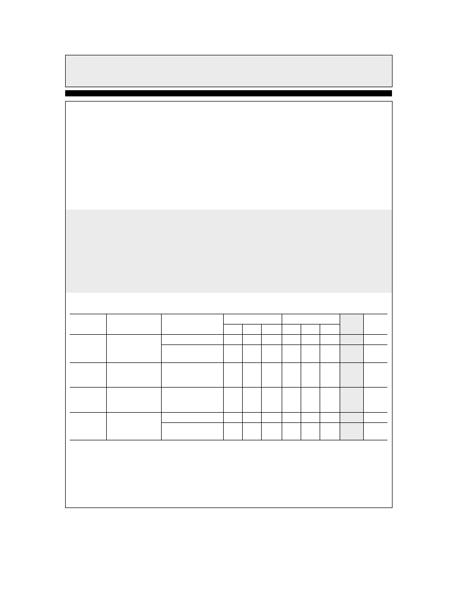
Absolute Maximum Ratings
VS
Supply Voltage
ELH0101 ELH0101A
g
22V
PD
Power Dissipation at TA e 25 C5W
Derate linearly at 25 CW
to zero at 150 C
PD
Power Dissipation at TC e 25 C
62W
Derate linearly at 2 CW
to zero at 150 C
Differential Input Voltage
ELH0101 ELH0101A
g
40V but k gVS
VIN
Input Voltage Range
ELH0101 ELH0101A
g
20V but k gVS
Peak Output Current (50 ms pulse)
5A
Output Short Circuit Duration
(within rated power dissipation
RSC e 035X TA e 25 C)
Continuous
TA
Operating Temperature Range
ELH0101 ELH0101A
b
55 Cto a125 C
TJ
Maximum Junction Temperature
150 C
TST
Storage Temperature
b
65 Cto a150 C
Lead Temperature
(Soldering 10 seconds)
300 C
Important Note
All parameters having MinMax specifications are guaranteed The Test Level column indicates the specific device testing actually
performed during production and Quality inspection Elantec performs most electrical tests using modern high-speed automatic test
equipment specifically the LTX77 Series system Unless otherwise noted all tests are pulsed tests therefore TJeTCeTA
Test Level
Test Procedure
I
100% production tested and QA sample tested per QA test plan QCX0002
II
100% production tested at TA e 25 C and QA sample tested at TA e 25 C
TMAX and TMIN per QA test plan QCX0002
III
QA sample tested per QA test plan QCX0002
IV
Parameter is guaranteed (but not tested) by Design and Characterization Data
V
Parameter is typical value at TA e 25 C for information purposes only
DC Electrical Characteristics (Note 1) V
S
e g
15V TA e 25 C VCM e 0V
Parameter
Description
Test Conditions
ELH0101
ELH0101A
Level
Test
Units
Min
Typ
Max
Min
Typ
Max
VOS
Input Offset
1
10
1
3
I
mV
Voltage
TMIN s TA s TMAX
15
7
I
mV
ELH0101
DVOS DPD
Change in Input
(Note 2)
Offset Voltage with
150
V
mVW
Dissipated Power
DVOS DT
Change in Input
Offset Voltage with
10
V
mV C
Temperature
IB
Input Bias Current
1000
300
I
pA
TA s TMAX
1000
300
I
nA
ELH0101
2
TD
is
23in
相關PDF資料 |
PDF描述 |
|---|---|
| ELH0101AK | Power Operational Amplifier |
| ELH0101K | Power Operational Amplifier |
| EM-SERIES | ASIC |
| EM08MR32UM | Dual Regulator-Synchronous Rectified Buck PWM and Linear Power Controller; Temperature Range: 0°C to 70°C; Package: 16-QFN |
| EM22003 | ACPI Regulator/Controller for Dual Channel DDR Memory Systems; Temperature Range: 0°C to 70°C; Package: 20-QFN |
相關代理商/技術參數(shù) |
參數(shù)描述 |
|---|---|
| ELH0101ACK | 制造商:未知廠家 制造商全稱:未知廠家 功能描述:Voltage-Feedback Operational Amplifier |
| ELH0101ACK/E+ | 制造商:未知廠家 制造商全稱:未知廠家 功能描述:Voltage-Feedback Operational Amplifier |
| ELH0101AK | 制造商:ELANTEC 制造商全稱:ELANTEC 功能描述:Power Operational Amplifier |
| ELH0101AK/883B | 制造商:E 功能描述: |
| ELH0101CK | 制造商:未知廠家 制造商全稱:未知廠家 功能描述:Voltage-Feedback Operational Amplifier |
發(fā)布緊急采購,3分鐘左右您將得到回復。