- 您現(xiàn)在的位置:買賣IC網(wǎng) > PDF目錄362652 > EL7586 (Intersil Corporation) TFT-LCD Power Supply PDF資料下載
參數(shù)資料
| 型號: | EL7586 |
| 廠商: | Intersil Corporation |
| 英文描述: | TFT-LCD Power Supply |
| 中文描述: | TFT - LCD的電源供應(yīng)器 |
| 文件頁數(shù): | 13/21頁 |
| 文件大小: | 772K |
| 代理商: | EL7586 |
13
FN9210.1
October 7, 2005
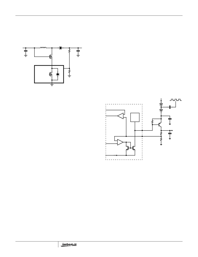
Cascaded MOSFET Application
A 20V N-channel MOSFET is integrated in the boost
regulator. For the applications where the output voltage is
greater than 20V, an external cascaded MOSFET is needed
as shown in Figure 27. The voltage rating of the external
MOSFET should be greater than V
BOOST
.
FIGURE 27. CASCADED MOSFET TOPOLOGY FOR HIGH
OUTPUT VOLTAGE APPLICATIONS
Linear-Regulator Controllers (V
ON
, V
LOGIC
, and
V
OFF
)
The EL7586 and EL7586A include three independent linear-
regulator controllers, in which two are positive output voltage
(V
ON
and V
LOGIC
), and one is negative. The V
ON
, V
OFF
,
and V
LOGIC
linear-regulator controller functional diagrams,
applications circuits are shown in Figures 28, 29, and 30
respectively.
Calculation of the Linear Regulator Base-Emitter
Resistors (R
BL
, R
BP
and R
BN
)
For the pass transistor of the linear regulator, low frequency
gain (Hfe) and unity gain freq. (f
T
) are usually specified in the
datasheet. The pass transistor adds a pole to the loop
transfer function at f
p
= f
T
/Hfe. Therefore, in order to
maintain phase margin at low frequency, the best choice for
a pass device is often a high frequency low gain switching
transistor. Further improvement can be obtained by adding a
base-emitter resistor R
BE
(R
BP
, R
BL
, R
BN
in the Functional
Block Diagram), which increase the pole frequency to:
f
p
= f
T
*(1+ Hfe *re/R
BE
)/Hfe, where re = KT/qIc. So choose
the lowest value R
BE
in the design as long as there is still
enough base current (I
B
) to support the maximum output
current (I
C
).
We will take as an example the V
LOGIC
linear regulator. If a
Fairchild FMMT549 PNP transistor is used as the external
pass transistor, Q5 in the application diagram, then for a
maximum V
LOGIC
operating requirement of 500mA the data
sheet indicates Hfe_min = 100.
The base-emitter saturation voltage is: Vbe_max = 1.25V
(note this is normally a Vbe ~ 0.7V, however, for the Q5
transistor an internal Darlington arrangement is used to
increase it's current gain, giving a 'base-emitter' voltage of
2 x V
BE
).
(Note that using a high current Darlington PNP transistor for
Q5 requires that V
IN
> V
LOGIC
+ 2V. Should a lower input
voltage be required, then an ordinary high gain PNP
transistor should be selected for Q5 so as to allow a lower
collector-emitter saturation voltage).
For the EL7586 and EL7586A, the minimum drive current is:
I_DRVL_min = 8mA
The minimum base-emitter resistor, R
BL
, can now be
calculated as:
R
BL
_min = V
BE
_max/(I_DRVL_min - Ic/Hfe_min) =
1.25V/(8mA - 500mA/100) = 417
This is the minimum value that can be used - so, we now
choose a convenient value greater than this minimum value;
say 500
. Larger values may be used to reduce quiescent
current, however, regulation may be adversely affected, by
supply noise if R
BL
is made too high in value.
FIGURE 28. V
ON
FUNCTIONAL BLOCK DIAGRAM
EL7586
EL7586A
FB
LX
V
BOOST
V
IN
-
GMP
+
-
+
36V
ESD
CLAMP
LDO_ON
PG_LDOP
1 : Np
FBP
DRVP
7k
R
BP
V
BOOST
0.1μF
0.1μF
CP (TO 36V)
20k
R
P2
R
P1
C
ON
V
ON
(TO 35V)
LX
0.9V
Q3
EL7586, EL7586A
相關(guān)PDF資料 |
PDF描述 |
|---|---|
| EL7586AILZ | TFT-LCD Power Supply |
| EL7586AILZ-T13 | TFT-LCD Power Supply |
| EL7586AILZ-T7 | TFT-LCD Power Supply |
| EL7630IWTZ | White LED Boost Regulator |
| EL7630ICZ-T7 | White LED Boost Regulator |
相關(guān)代理商/技術(shù)參數(shù) |
參數(shù)描述 |
|---|---|
| EL7586_06 | 制造商:INTERSIL 制造商全稱:Intersil Corporation 功能描述:TFT-LCD Power Supply |
| EL7586A | 制造商:INTERSIL 制造商全稱:Intersil Corporation 功能描述:TFT-LCD Power Supply |
| EL7586AILZ | 功能描述:直流/直流開關(guān)調(diào)節(jié)器 EL7586AILZ TFT-LCD PWR SUPY RoHS:否 制造商:International Rectifier 最大輸入電壓:21 V 開關(guān)頻率:1.5 MHz 輸出電壓:0.5 V to 0.86 V 輸出電流:4 A 輸出端數(shù)量: 最大工作溫度: 安裝風(fēng)格:SMD/SMT 封裝 / 箱體:PQFN 4 x 5 |
| EL7586AILZ-T13 | 功能描述:直流/直流開關(guān)調(diào)節(jié)器 EL7586AILZ TFT-LCD P PWR SUPY RoHS:否 制造商:International Rectifier 最大輸入電壓:21 V 開關(guān)頻率:1.5 MHz 輸出電壓:0.5 V to 0.86 V 輸出電流:4 A 輸出端數(shù)量: 最大工作溫度: 安裝風(fēng)格:SMD/SMT 封裝 / 箱體:PQFN 4 x 5 |
| EL7586AILZ-T7 | 功能描述:直流/直流開關(guān)調(diào)節(jié)器 EL7586AILZ TFT-LCD PWR SUPY RoHS:否 制造商:International Rectifier 最大輸入電壓:21 V 開關(guān)頻率:1.5 MHz 輸出電壓:0.5 V to 0.86 V 輸出電流:4 A 輸出端數(shù)量: 最大工作溫度: 安裝風(fēng)格:SMD/SMT 封裝 / 箱體:PQFN 4 x 5 |
發(fā)布緊急采購,3分鐘左右您將得到回復(fù)。