- 您現(xiàn)在的位置:買賣IC網(wǎng) > PDF目錄362638 > EL5165IWZ-T7A (INTERSIL CORP) 600MHz Current Feedback Amplifiers with Enable PDF資料下載
參數(shù)資料
| 型號(hào): | EL5165IWZ-T7A |
| 廠商: | INTERSIL CORP |
| 元件分類: | 音頻/視頻放大 |
| 英文描述: | 600MHz Current Feedback Amplifiers with Enable |
| 中文描述: | 1 CHANNEL, VIDEO AMPLIFIER, PDSO5 |
| 封裝: | ROHS COMPLIANT, SOT-23, 6 PIN |
| 文件頁(yè)數(shù): | 11/12頁(yè) |
| 文件大小: | 411K |
| 代理商: | EL5165IWZ-T7A |
11
choice for driving isolation transformers in
telecommunications applications.
Driving Cables and Capacitive Loads
When used as a cable driver, double termination is always
recommended for reflection-free performance. For those
applications, the back-termination series resistor will
decouple the EL5164, EL5165, and EL5364 from the cable
and allow extensive capacitive drive. However, other
applications may have high capacitive loads without a back-
termination resistor. In these applications, a small series
resistor (usually between 5
and 50
) can be placed in
series with the output to eliminate most peaking. The gain
resistor (R
G
) can then be chosen to make up for any gain
loss which may be created by this additional resistor at the
output. In many cases it is also possible to simply increase
the value of the feedback resistor (R
F
) to reduce the
peaking.
Current Limiting
The EL5164, EL5165, and EL5364 have no internal current-
limiting circuitry. If the output is shorted, it is possible to
exceed the Absolute Maximum Rating for output current or
power dissipation, potentially resulting in the destruction of
the device.
Power Dissipation
With the high output drive capability of the EL5164, EL5165,
and EL5364, it is possible to exceed the 125°C Absolute
Maximum junction temperature under certain very high load
current conditions. Generally speaking when R
L
falls below
about 25
, it is important to calculate the maximum junction
temperature (T
JMAX
) for the application to determine if
power supply voltages, load conditions, or package type
need to be modified for the EL5164, EL5165, and EL5364 to
remain in the safe operating area. These parameters are
calculated as follows:
where:
T
MAX
= Maximum ambient temperature
θ
JA
= Thermal resistance of the package
n = Number of amplifiers in the package
PD
MAX
= Maximum power dissipation of each amplifier in
the package
PD
MAX
for each amplifier can be calculated as follows:
where:
V
S
= Supply voltage
I
SMAX
= Maximum supply current of 1A
V
OUTMAX
= Maximum output voltage (required)
R
L
= Load resistance
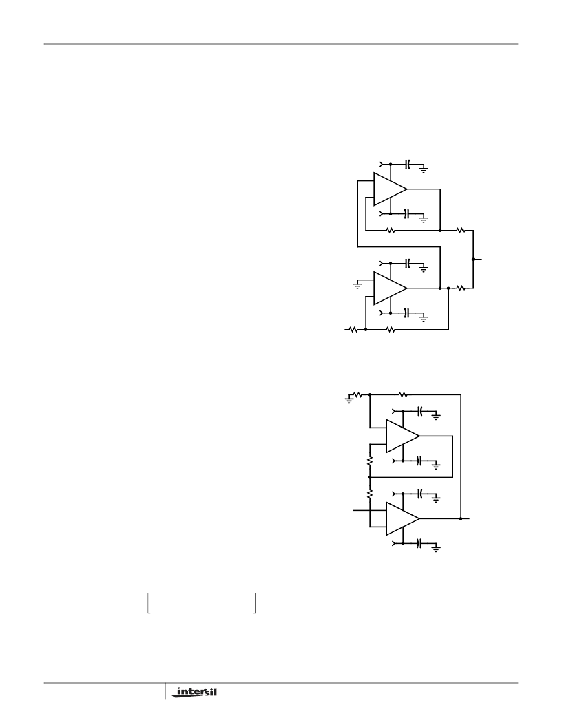
Typical Application Circuits
FIGURE 23. INVERTING 200mA OUTPUT CURRENT
DISTRIBUTION AMPLIFIER
FIGURE 24. FAST-SETTLING PRECISION AMPLIFIER
T
JMAX
T
MAX
θ
JA
n
PD
MAX
×
×
(
)
+
=
PD
MAX
2
(
V
S
I
SMAX
)
V
S
(
V
OUTMAX
)
V
L
----------------------------
×
–
+
×
×
=
IN+
IN-
V
S
+
V
S
-
OUT
IN+
IN-
V
S
+
V
S
-
OUT
0.1μF
+5V
0.1μF
-5V
375
5
5
375
375
V
OUT
V
IN
0.1μF
0.1μF
+5V
-5V
IN+
IN-
V
S
+
V
S
-
OUT
IN+
IN-
V
S
+
V
S
-
OUT
0.1μF
+5V
0.1μF
-5V
0.1μF
0.1μF
375
375
375
375
V
OUT
V
IN
+5V
-5V
EL5164, EL5165, EL5364
相關(guān)PDF資料 |
PDF描述 |
|---|---|
| EL5164 | 600MHz Current Feedback Amplifiers with Enable |
| EL5164IS | 600MHz Current Feedback Amplifiers with Enable |
| EL5164ISZ-T13 | 600MHz Current Feedback Amplifiers with Enable |
| EL5364ISZ-T13 | 600MHz Current Feedback Amplifiers with Enable |
| EL5364ISZ | 600MHz Current Feedback Amplifiers with Enable |
相關(guān)代理商/技術(shù)參數(shù) |
參數(shù)描述 |
|---|---|
| EL5166 | 制造商:INTERSIL 制造商全稱:Intersil Corporation 功能描述:1.4GHz Current Feedback Amplifiers with Enable |
| EL5166_05 | 制造商:INTERSIL 制造商全稱:Intersil Corporation 功能描述:1.4GHz Current Feedback Amplifiers with Enable |
| EL5166_07 | 制造商:INTERSIL 制造商全稱:Intersil Corporation 功能描述:1.4GHz Current Feedback Amplifiers with Enable |
| EL516-60-1 | 制造商:未知廠家 制造商全稱:未知廠家 功能描述:Logic IC |
| EL516-6-1 | 制造商:未知廠家 制造商全稱:未知廠家 功能描述:Logic IC |
發(fā)布緊急采購(gòu),3分鐘左右您將得到回復(fù)。