- 您現(xiàn)在的位置:買賣IC網(wǎng) > PDF目錄378593 > DSP201JP 16-bit fixed point DSP with Flash PDF資料下載
參數(shù)資料
| 型號: | DSP201JP |
| 元件分類: | 數(shù)字信號處理 |
| 英文描述: | 16-bit fixed point DSP with Flash |
| 中文描述: | 具有閃存的 16 位定點 DSP |
| 文件頁數(shù): | 13/19頁 |
| 文件大?。?/td> | 106K |
| 代理商: | DSP201JP |
DSP201/202
13
APPLICATIONS
USING PARALLEL PORTS
WITH THE DSP201 OR DSP202
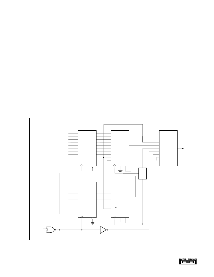
Figure 5 shows a circuit for converting parallel outputs into
the serial data stream required by the DSP201, and meets the
requirements for timing signals. Doubling this circuit allows
the DSP202 to be driven from a 32-bit parallel port. In most
applications, this circuit can be easily incorporated into gate
arrays or other programmed logic circuits already used in the
system, since the extra gate count is not high.
DEGLITCHING
Particularly in high resolution D/A converters, changing
input codes may cause glitching on the output that exces-
sively corrupts the dynamic purity of an output signal. The
DSP201 and DSP202 are designed to minimize output
glitching, and all of the performance specifications and
typical performance curves are based on tests with no extra
deglitching circuitry. In particular, the guaranteed Signal-to-
(Noise + Distortion) performance would be impossible to
attain with any significant glitching.
COMPLETE ANALOG INPUT/OUTPUT SYSTEM
The DSP201 or DSP202 can be paired with the Burr-Brown
DSP101 or DSP102 analog-to-digital converter to provide
both analog input and analog output for a complete digital
signal processing system. The DSP101 and DSP102 are
respectively single and dual channel 200kHz sampling A/Ds
with easy to use interfacing logic that complement the
DSP201 and DSP202. Figure 6 shows a single channel
analog input and output system based on a DSP201 and a
DSP101, and the minimal connections required to interface
to a DSP IC. A pair of channels can be implemented using
a single DSP202 and a single DSP102, either with two
separate DSP ICs, with a single DSP IC with dual serial
input and output channels, or a single DSP IC capable of 32-
bit words in the Cascade Mode.
For maximum flexibility in system design, the DSP201 or
DSP202 D/As can be updated at a different rate than the
conversion rate used on the DSP101 or DSP102 A/Ds, and
either or both of these rates can be asynchronous to the
clocks used with the DSP IC.
FIGURE 5. Driving the DSP201 from a 16-Bit Parallel Port.
8D
7D
6D
5D
4D
3D
2D
1D
18
17
14
13
8
7
4
3
74LS32
74LS04
2
1
6
WR
PORTAO
4
5
19
16
15
12
9
6
5
2
8Q
7Q
6Q
5Q
4Q
3Q
2Q
1Q
CK
OE
H
G
F
E
D
C
B
A
S/L
SI
C
14
12
11
10
5
4
3
2
15
1
13
QH
CI
CL
74LS374
74LS166
11
1
7
6
9
+5V
TTL
Bit
Clock
SYNC
SIN
XCLK
CONV
SSF
SWL
11
13
12
15
9
10
21
VOUT
DSP201
±3V
Analog
Output
8D
7D
6D
5D
4D
3D
2D
1D
18
17
14
13
8
7
4
3
19
16
15
12
9
6
5
2
8Q
7Q
6Q
5Q
4Q
3Q
2Q
1Q
CK
OE
H
G
F
E
D
C
B
A
S/L
SI
C
14
12
11
10
5
4
3
2
15
1
13
QH
CI
CL
74LS374
74LS166
11
1
7
6
9
+5V
D0
D1
D2
D3
D4
D5
D6
D7
D8
D9
D10
D11
D12
D13
D14
D15
LSB
MSB
+5V
相關(guān)PDF資料 |
PDF描述 |
|---|---|
| DSP201KP | 16-bit fixed point DSP with Flash |
| DSP202 | 16-bit fixed point DSP with Flash |
| DSP202JP | 16-bit fixed point DSP with Flash |
| DSP202KP | 16-bit fixed point DSP with Flash |
| DSP56004FJ81 | SYMPHONY AUDIO DSP FAMILY 24-BIT DIGITAL SIGNAL PROCESSORS |
相關(guān)代理商/技術(shù)參數(shù) |
參數(shù)描述 |
|---|---|
| DSP201KP | 制造商:BB 制造商全稱:BB 功能描述:DSP-Compatible Single/Dual DIGITAL-TO-ANALOG CONVERTERS |
| DSP-201M | 制造商:MITSUBISHI 制造商全稱:Mitsubishi Electric Semiconductor 功能描述:DIA SURGE SUPPRESSOR (DSS) |
| DSP202 | 制造商:BB 制造商全稱:BB 功能描述:DSP-Compatible Single/Dual DIGITAL-TO-ANALOG CONVERTERS |
| DSP-202 | 制造商:SYNERGY 制造商全稱:SYNERGY MICROWAVE CORPORATION 功能描述:POWER DIVIDERS 0ì : 2-WAY |
| DSP202JP | 制造商:BB 制造商全稱:BB 功能描述:DSP-Compatible Single/Dual DIGITAL-TO-ANALOG CONVERTERS |
發(fā)布緊急采購,3分鐘左右您將得到回復。