- 您現(xiàn)在的位置:買賣IC網(wǎng) > PDF目錄11542 > DS21Q42T (Maxim Integrated Products)IC FRAMER ENHANCED T1 4X 128TQFP PDF資料下載
參數(shù)資料
| 型號(hào): | DS21Q42T |
| 廠商: | Maxim Integrated Products |
| 文件頁數(shù): | 75/116頁 |
| 文件大小: | 0K |
| 描述: | IC FRAMER ENHANCED T1 4X 128TQFP |
| 標(biāo)準(zhǔn)包裝: | 72 |
| 控制器類型: | T1 調(diào)幀器 |
| 接口: | 并行/串行 |
| 電源電壓: | 2.97 V ~ 3.63 V |
| 電流 - 電源: | 75mA |
| 工作溫度: | 0°C ~ 70°C |
| 安裝類型: | 表面貼裝 |
| 封裝/外殼: | 128-LQFP |
| 供應(yīng)商設(shè)備封裝: | 128-LQFP(14x20) |
| 包裝: | 管件 |
第1頁第2頁第3頁第4頁第5頁第6頁第7頁第8頁第9頁第10頁第11頁第12頁第13頁第14頁第15頁第16頁第17頁第18頁第19頁第20頁第21頁第22頁第23頁第24頁第25頁第26頁第27頁第28頁第29頁第30頁第31頁第32頁第33頁第34頁第35頁第36頁第37頁第38頁第39頁第40頁第41頁第42頁第43頁第44頁第45頁第46頁第47頁第48頁第49頁第50頁第51頁第52頁第53頁第54頁第55頁第56頁第57頁第58頁第59頁第60頁第61頁第62頁第63頁第64頁第65頁第66頁第67頁第68頁第69頁第70頁第71頁第72頁第73頁第74頁當(dāng)前第75頁第76頁第77頁第78頁第79頁第80頁第81頁第82頁第83頁第84頁第85頁第86頁第87頁第88頁第89頁第90頁第91頁第92頁第93頁第94頁第95頁第96頁第97頁第98頁第99頁第100頁第101頁第102頁第103頁第104頁第105頁第106頁第107頁第108頁第109頁第110頁第111頁第112頁第113頁第114頁第115頁第116頁
DS21Q42
61 of 116
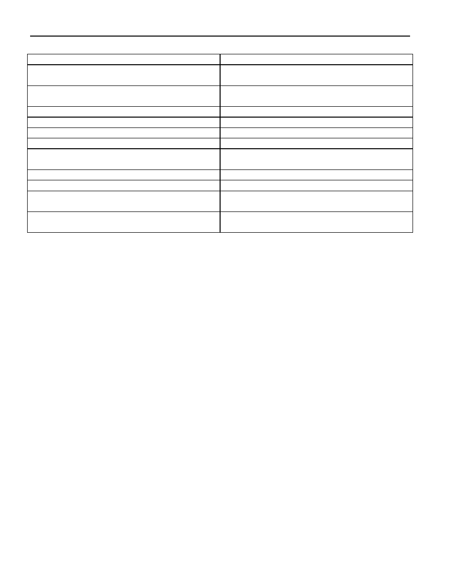
Table 15-1. HDLC/BOC CONTROLLER REGISTER LIST
NAME
FUNCTION
HDLC Control Register (HCR)
general control over the HDLC and BOC
controllers
HDLC Status Register (HSR)
key status information for both transmit and receive
directions
HDLC Interrupt Mask Register (HIMR)
allows/stops status bits to/from causing an interrupt
Receive HDLC Information Register (RHIR)
status information on receive HDLC controller
Receive BOC Register (RBOC)
status information on receive BOC controller
Receive HDLC FIFO Register (RHFR)
access to 64–byte HDLC FIFO in receive direction
Receive HDLC DS0 Control Register 1 (RDC1)
Receive HDLC DS0 Control Register 2 (RDC2)
controls the HDLC function when used on DS0
channels
Transmit HDLC Information Register (THIR)
status information on transmit HDLC controller
Transmit BOC Register (TBOC)
enables/disables transmission of BOC codes
Transmit HDLC FIFO Register (THFR)
access to 64–byte HDLC FIFO in transmit
direction
Transmit HDLC DS0 Control Register 1 (TDC1)
Transmit HDLC DS0 Control Register 2 (TDC2)
controls the HDLC function when used on DS0
channels
15.1.2 Status Register for the HDLC
Four of the HDLC/BOC controller registers (HSR, RHIR, RBOC, and THIR) provide status information.
When a particular event has occurred (or is occurring), the appropriate bit in one of these four registers
will be set to a one. Some of the bits in these four HDLC status registers are latched and some are real
time bits that are not latched. Section 15.1.4 contains register descriptions that list which bits are latched
and which are not. With the latched bits, when an event occurs and a bit is set to a one, it will remain set
until the user reads that bit. The bit will be cleared when it is read and it will not be set again until the
event has occurred again. The real time bits report the current instantaneous conditions that are occurring
and the history of these bits is not latched.
Like the other status registers in the DS21Q42, the user will always proceed a read of any of the four
registers with a write. The byte written to the register will inform the DS21Q42 which of the latched bits
the user wishes to read and have cleared (the real time bits are not affected by writing to the status
register). The user will write a byte to one of these registers, with a one in the bit positions he or she
wishes to read and a zero in the bit positions he or she does not wish to obtain the latest information on.
When a one is written to a bit location, the read register will be updated with current value and it will be
cleared. When a zero is written to a bit position, the read register will not be updated and the previous
value will be held. A write to the status and information registers will be immediately followed by a read
of the same register. The read result should be logically AND’ed with the mask byte that was just written
and this value should be written back into the same register to insure that bit does indeed clear. This
second write step is necessary because the alarms and events in the status registers occur asynchronously
in respect to their access via the parallel port. This write–read–write (for polled driven access) or
write-read (for interrupt driven access) scheme allows an external microcontroller or microprocessor to
individually poll certain bits without disturbing the other bits in the register. This operation is key in
controlling the DS21Q42 with higher–order software languages.
相關(guān)PDF資料 |
PDF描述 |
|---|---|
| V72A28C400B | CONVERTER MOD DC/DC 28V 400W |
| DS21Q44T | IC FRAMER ENHANCED E1 4X 128TQFP |
| V72A24C400BF | CONVERTER MOD DC/DC 24V 400W |
| XCCACE-TQ144I | IC ACE CONTROLLER CHIP |
| VI-21W-IY-B1 | CONVERTER MOD DC/DC 5.5V 50W |
相關(guān)代理商/技術(shù)參數(shù) |
參數(shù)描述 |
|---|---|
| DS21Q42T+ | 功能描述:網(wǎng)絡(luò)控制器與處理器 IC Enhanced Quad T1 Framer RoHS:否 制造商:Micrel 產(chǎn)品:Controller Area Network (CAN) 收發(fā)器數(shù)量: 數(shù)據(jù)速率: 電源電流(最大值):595 mA 最大工作溫度:+ 85 C 安裝風(fēng)格:SMD/SMT 封裝 / 箱體:PBGA-400 封裝:Tray |
| DS21Q42TN | 功能描述:網(wǎng)絡(luò)控制器與處理器 IC Enhanced Quad T1 Framer RoHS:否 制造商:Micrel 產(chǎn)品:Controller Area Network (CAN) 收發(fā)器數(shù)量: 數(shù)據(jù)速率: 電源電流(最大值):595 mA 最大工作溫度:+ 85 C 安裝風(fēng)格:SMD/SMT 封裝 / 箱體:PBGA-400 封裝:Tray |
| DS21Q43A | 制造商:DALLAS 制造商全稱:Dallas Semiconductor 功能描述:Quad E1 Framer |
| DS21Q43AT | 功能描述:網(wǎng)絡(luò)控制器與處理器 IC Quad E1 Framer RoHS:否 制造商:Micrel 產(chǎn)品:Controller Area Network (CAN) 收發(fā)器數(shù)量: 數(shù)據(jù)速率: 電源電流(最大值):595 mA 最大工作溫度:+ 85 C 安裝風(fēng)格:SMD/SMT 封裝 / 箱體:PBGA-400 封裝:Tray |
| DS21Q43AT+ | 功能描述:網(wǎng)絡(luò)控制器與處理器 IC Quad E1 Framer RoHS:否 制造商:Micrel 產(chǎn)品:Controller Area Network (CAN) 收發(fā)器數(shù)量: 數(shù)據(jù)速率: 電源電流(最大值):595 mA 最大工作溫度:+ 85 C 安裝風(fēng)格:SMD/SMT 封裝 / 箱體:PBGA-400 封裝:Tray |
發(fā)布緊急采購,3分鐘左右您將得到回復(fù)。